
 E-mail Alert
 RSS
RSS
| Citation: |
Liu Z X, Jiang M L, Hu Y L, Lin F, Shen B et al. Scanning cathodoluminescence microscopy: applications in semiconductor and metallic nanostructures. Opto-Electron Adv 1, 180007 (2018). doi: 10.29026/oea.2018.180007

|
Scanning cathodoluminescence microscopy: applications in semiconductor and metallic nanostructures
-
Abstract
Cathodoluminescence (CL) as a radiative light produced by an electron beam exciting a luminescent material, has been widely used in imaging and spectroscopic detection of semiconductor, mineral and biological samples with an ultrahigh spatial resolution. Conventional CL spectroscopy shows an excellent performance in characterization of traditional material luminescence, such as spatial composition variations and fluorescent displays. With the development of nanotechnology, advances of modern microscopy enable CL technique to obtain deep valuable insight of the testing sample, and further extend its applications in the material science, especially for opto-electronic investigations at nanoscale. In this article, we review the study of CL microscopy applied in semiconductor nanostructures for the dislocation, carrier diffusion, band structure, doping level and exciton recombination. Then advantages of CL in revealing and manipulating surface plasmon resonances of metallic nanoantennas are discussed. Finally, the challenge of CL technology is summarized, and potential CL applications for the future opto-electronic study are proposed.-
Keywords:
- cathodoluminescence /
- microscopy /
- semiconductor /
- metallic nanostructures /
- surface plasmons
-

-
References
[1] Coenen T, Haegel N M. Cathodoluminescence for the 21st century: Learning more from light. Appl Phys Rev 4, 031103 (2017). doi: 10.1063/1.4985767 [2] Pohl D W, Fischer U C, Dürig U T. Scanning near-field optical microscopy (Snom). J Microsc 152, 853–861 (1988). doi: 10.1111/jmi.1988.152.issue-3 [3] Schieber J, Krinsley D, Riciputi L. Diagenetic origin of quartz silt in mudstones and implications for silica cycling. Nature 406, 981–985 (2000). doi: 10.1038/35023143 [4] Pratesi G, Giudice A L, Vishnevsky S, Manfredotti C, Cipriani C. Cathodoluminescence investigations on the Popigai, Ries, and Lappajarvi impact diamonds. Am Mineral 88, 1778–1787 (2003). doi: 10.2138/am-2003-11-1218 [5] Pennycook S J. Investigating the optical properties of dislocations by scanning transmission electron microscopy. Scanning 30, 287–298 (2008). doi: 10.1002/sca.v30:4 [6] Watanabe K, Nagata T, Wakayama Y, Sekiguchi T, Erdélyi R et al. Band-Gap Deformation Potential and Elasticity Limit of Semiconductor Free-Standing Nanorods Characterized in Situ by Scanning Electron Microscope-Cathodoluminescence Nanospectroscopy. ACS Nano 9, 2989–3001 (2015). doi: 10.1021/nn507159u [7] Brenny B J M, Coenen T, Polman A. Quantifying coherent and incoherent cathodoluminescence in semiconductors and metals. J Appl Phys 115, 244307 (2014). doi: 10.1063/1.4885426 [8] Storm K, Halvardsson F, Heurlin M, Lindgren D, Gustafsson A et al. Spatially resolved Hall effect measurement in a single semiconductor nanowire. Nat Nanotechnol 7, 718–722 (2012). doi: 10.1038/nnano.2012.190 [9] Niioka H, Furukawa T, Ichimiya M, Ashida M, Araki T et al. Multicolor Cathodoluminescence Microscopy for Biological Imaging with Nanophosphors. Appl Phys Express 4, 112402 (2011). doi: 10.1143/APEX.4.112402 [10] Barnett W A, Wise M L H, Jones E C. Cathodoluminescence of biological molecules, macromolecules and cells. J Microsc 105, 299–303 (1975). doi: 10.1111/jmi.1975.105.issue-3 [11] Coenen T, Brenny B J M, Vesseur E J, Polman A. Cathodoluminescence microscopy: Optical imaging and spectroscopy with deep-subwavelength resolution. MRS Bull 40, 359–365 (2015). doi: 10.1557/mrs.2015.64 [12] Kociak M, Zagonel L F. Cathodoluminescence in the scanning transmission electron microscope. Ultramicroscopy 176, 112–131 (2017). doi: 10.1016/j.ultramic.2017.03.014 [13] Gotze J. Potential of cathodoluminescence (CL) microscopy and spectroscopy for the analysis of minerals and materials. Anal Bioanal Chem 374, 703–708 (2002). doi: 10.1007/s00216-002-1461-1 [14] Sauer R, Sternschulte H, Wahl S, Thonke K, Anthony T R. Revised fine splitting of excitons in diamond. Phys Rev Lett 84, 4172–4175 (2000). doi: 10.1103/PhysRevLett.84.4172 [15] Koizumi S, Watanabe K, Hasegawa M, Kanda H. Ultraviolet emission from a diamond pn junction. Science 292, 1899–1901 (2001). doi: 10.1126/science.1060258 [16] Li G G, Geng D L, Shang M M, Peng C, Cheng Z Y et al. Tunable luminescence of Ce3+/Mn2+-coactivated Ca2Gd8(SiO4)6O2 through energy transfer and modulation of excitation: potential single-phase white/yellow-emitting phosphors. J Mater Chem 21, 13334 (2011). doi: 10.1039/c1jm11650a [17] Edwards P R, Martin R W. Cathodoluminescence nano-characterization of semiconductors. Semicond Sci Tech 26, 064005 (2011). doi: 10.1088/0268-1242/26/6/064005 [18] Dierre B, Yuan X L, Sekiguchi T. Low-energy cathodoluminescence microscopy for the characterization of nanostructures. Sci Technol Adv Mater 11, 043001 (2010). doi: 10.1088/1468-6996/11/4/043001 [19] Leto A, Pezzotti G. Cathodoluminescence study of off-stoichiometry and residual stresses in advanced dielectrics and related devices. Phys Status Solidi A 208, 1119–1126 (2011). doi: 10.1002/pssa.v208.5 [20] Zhai T Y, Fang X S, Bando Y, Dierre B, Liu B D et al. Characterization, cathodoluminescence, and field-emission properties of morphology-tunable CdS micro/nanostructures. Adv Funct Mater 19, 2423–2430 (2009). doi: 10.1002/adfm.v19:15 [21] Gautam U K, Panchakarla L S, Dierre B, Fang X S, Bando Y et al. Solvothermal Synthesis, Cathodoluminescence, and Field-Emission Properties of Pure and N-Doped ZnO Nanobullets. Adv Funct Mater 19, 131–140 (2009). doi: 10.1002/adfm.v19:1 [22] Yacobi B G, Holt D B. Cathodoluminescence scanning electron microscopy of semiconductors. J Appl Phys 59, R1–R24 (1986). doi: 10.1063/1.336491 [23] Shubina T V, Ivanov S V, Jmerik V N, Solnyshkov D D, Vekshin V A et al. Mie resonances, infrared emission, and the band gap of InN. Phys Rev Lett 92, 117407 (2004). doi: 10.1103/PhysRevLett.92.117407 [24] Schue L, Berini B, Betz A C, Placais B, Ducastelle F et al. Dimensionality effects on the luminescence properties of hBN. Nanoscale 8, 6986–6993 (2016). doi: 10.1039/C6NR01253A [25] Vesseur E J R, Aizpurua J, Coenen T, Reyes-Coronado A, Batson P E et al. Plasmonic excitation and manipulation with an electron beam. MRS Bull 37, 752–760 (2012). doi: 10.1557/mrs.2012.174 [26] Barnes W L, Dereux A, Ebbesen T W. Surface plasmon subwavelength optics. Nature 424, 824–830 (2003). doi: 10.1038/nature01937 [27] Pendry J B, Martin-Moreno L, Garcia-Vidal F J. Mimicking surface plasmons with structured surfaces. Science 305, 847–848 (2004). doi: 10.1126/science.1098999 [28] Nelayah J, Kociak M, Stéphan O, García de Abajo F J, Tencé M et al. Mapping surface plasmons on a single metallic nanoparticle. Nat Phys 3, 348–353 (2007). doi: 10.1038/nphys575 [29] Choi H, Pile D F P, Nam S, Bartal G, Zhang X. Compressing surface plasmons for nano-scale optical focusing. Opt Express 17, 7519–7524 (2009). doi: 10.1364/OE.17.007519 [30] Dionne J A, Sweatlock L A, Atwater H A, Polman A. Plasmon slot waveguides: Towards chip-scale propagation with subwavelength-scale localization. Phys Rev B 73, 035407 (2006). doi: 10.1103/PhysRevB.73.035407 [31] Yamamoto N, Bhunia S, Watanabe Y. Polarized cathodoluminescence study of InP nanowires by transmission electron microscopy. Appl Phys Lett 88, 153106 (2006). doi: 10.1063/1.2168043 [32] Vesseur E J R, Coenen T, Caglayan H, Engheta N, Polman A. Experimental verification of n=0 structures for visible light. Phys Rev Lett 110, 013902 (2013). doi: 10.1103/PhysRevLett.110.013902 [33] Narvaez A C, Weppelman I G C, Moerland R J, Liv N, Zonnevylle A C et al. Cathodoluminescence Microscopy of nanostructures on glass substrates. Opt Express 21, 29968–29978 (2013). doi: 10.1364/OE.21.029968 [34] Aubry A, Lei D Y, Fernandez-Dominguez A I, Sonnefraud Y, Maier S A et al. Plasmonic light-harvesting devices over the whole visible spectrum. Nano Lett 10, 2574–2579 (2010). doi: 10.1021/nl101235d [35] Ropers C, Neacsu C C, Elsaesser T, Albrecht M, Raschke M B et al. Grating-coupling of surface plasmons onto metallic tips: a nanoconfined light source. Nano Lett 7, 2784–2788 (2007). doi: 10.1021/nl071340m [36] Cao Q, Lalanne P. Negative role of surface plasmons in the transmission of metallic gratings with very narrow slits. Phys Rev Lett 88, 057403 (2002). doi: 10.1103/PhysRevLett.88.057403 [37] Bashevoy M V, Jonsson F, MacDonald K F, Chen Y, Zheludev N I. Hyperspectral imaging of plasmonic nanostructures with nanoscale resolution. Opt Express 15, 11313–11320 (2007). doi: 10.1364/OE.15.011313 [38] Vesseur E J R, de Waele R, Kuttge M, Polman A. Direct observation of plasmonic modes in Au nanowires using high-resolution cathodoluminescence spectroscopy. Nano Lett 7, 2843–2846 (2007). doi: 10.1021/nl071480w [39] Kuttge M, de Abajo F J G, Polman A. Ultrasmall mode volume plasmonic nanodisk resonators. Nano Lett 10, 1537–1541 (2010). doi: 10.1021/nl902546r [40] Hofmann C E, Vesseur E J R, Sweatlock L A, Lezec H J, de Abajo F J G et al. Plasmonic modes of annular nanoresonators imaged by spectrally resolved cathodoluminescence. Nano Lett 7, 3612–3617 (2007). doi: 10.1021/nl071789f [41] Chaturvedi P, Hsu K H, Kumar A, Fung K H, Mabon J C et al. Imaging of plasmonic modes of silver nanoparticles using high-resolution cathodoluminescence spectroscopy. ACS Nano 3, 2965–2974 (2009). doi: 10.1021/nn900571z [42] Day J K, Large N, Nordlander P, Halas N J. Standing wave plasmon modes interact in an antenna-coupled nanowire. Nano Lett 15, 1324–1330 (2015). doi: 10.1021/nl5045428 [43] Arango F B, Coenen T, Koenderink A F. Underpinning Hybridization Intuition for Complex Nanoantennas by Magnetoelectric Quadrupolar Polarizability Retrieval. ACS Photonics 1, 444–453 (2014). doi: 10.1021/ph5000133 [44] Acar H, Coenen T, Polman A, Kuipers L K. Dispersive Ground Plane Core-Shell Type Optical Monopole Antennas Fabricated with Electron Beam Induced Deposition. ACS Nano 6, 8226–8232 (2012). doi: 10.1021/nn302907j [45] Koh A L, Bao K, Khan I, Smith W E, Kothleitner G et al. Electron energy-loss spectroscopy (EELS) of surface plasmons in single silver nanoparticles and dimers: influence of beam damage and mapping of dark modes. ACS Nano 3, 3015–3022 (2009). doi: 10.1021/nn900922z [46] Flauraud V, Bernasconi G D, Butet J, Alexander D T L, Martin O J F et al. Mode Coupling in Plasmonic Heterodimers Probed with Electron Energy Loss Spectroscopy. ACS Nano 11, 3485–3495 (2017). doi: 10.1021/acsnano.6b08589 [47] Sun Q, Ueno K, Yu H, Kubo A, Matsuo Y et al. Direct imaging of the near field and dynamics of surface plasmon resonance on gold nanostructures using photoemission electron microscopy. Light-Sci Appl 2, e118–e118 (2013). doi: 10.1038/lsa.2013.74 [48] Sun Q, Yu H, Ueno K, Kubo A, Matsuo Y et al. Dissecting the Few-Femtosecond Dephasing Time of Dipole and Quadrupole Modes in Gold Nanoparticles Using Polarized Photoemission Electron Microscopy. ACS Nano 10, 3835–3842 (2016). doi: 10.1021/acsnano.6b00715 [49] Toth M, Phillips M R. Monte Carlo modeling of cathodoluminescence generation using electron energy loss curves. Scanning 20, 425–432 (1998). [50] Titchmarsh J M, Booker G R, Harding W, Wight D R. Carrier recombination at dislocations in epitaxial gallium phosphide layers. J Mater Sci Mater Med 12, 341–346 (1977). doi: 10.1007/BF00566276 [51] Nakagawa K, Maeda K, Takeuchi S. Observation of dislocations in cadmium telluride by cathodoluminescence microscopy. Appl Phys Lett 34, 574 (1979). doi: 10.1063/1.90871 [52] Zarem H A, Sercel P C, Lebens J A, Eng L E, Yariv A et al. Direct determination of the ambipolar diffusion length in GaAs/AlGaAs heterostructures by cathodoluminescence. Appl Phys Lett 55, 1647–1649 (1989). doi: 10.1063/1.102226 [53] Merano M, Sonderegger S, Crottini A, Collin S, Renucci P et al. Probing carrier dynamics in nanostructures by picosecond cathodoluminescence. Nature 438, 479–482 (2005). doi: 10.1038/nature04298 [54] Chen H L, Himwas C, Scaccabarozzi A, Rale P, Oehler F et al. Determination of n-Type Doping Level in Single GaAs Nanowires by Cathodoluminescence. Nano Lett 17, 6667–6675 (2017). doi: 10.1021/acs.nanolett.7b02620 [55] Kaganer V M, Sabelfeld K K, Brandt O. Piezoelectric field, exciton lifetime, and cathodoluminescence intensity at threading dislocations in GaN{0001}. Appl Phys Lett 112, 122101 (2018). doi: 10.1063/1.5022170 [56] Pozina G, Ciechonski R, Bi Z X, Samuelson L, Monemar B. Dislocation related droop in InGaN/GaN light emitting diodes investigated via cathodoluminescence. Appl Phys Lett 107, 251106 (2015). doi: 10.1063/1.4938208 [57] Jahn U, Miguel-Sánchez J, Flissikowski T, Grahn H T, Hey R et al. Carrier diffusion lengths in (In, Ga)(As, N)/GaAs quantum wells studied by spatially resolved cathodoluminescence. Phys Status Solidi C 3, 627–630 (2006). doi: 10.1002/(ISSN)1610-1642 [58] Pauc N, Phillips M R, Aimez V, Drouin D. Carrier recombination near threading dislocations in GaN epilayers by low voltage cathodoluminescence. Appl Phys Lett 89, 161905 (2006). doi: 10.1063/1.2357881 [59] Jahn U, Ristić J, Calleja E. Cathodoluminescence spectroscopy and imaging of GaN∕(Al, Ga)N nanocolumns containing quantum disks. Appl Phys Lett 90, 161117 (2007). doi: 10.1063/1.2724913 [60] Li Z W, Li Y, Han T Y, Wang X L, Yu Y et al. Tailoring MoS2 Exciton-Plasmon Interaction by Optical Spin-Orbit Coupling. ACS Nano 11, 1165–1171 (2017). doi: 10.1021/acsnano.6b06834 [61] Li Z W, Xiao Y D, Gong Y J, Wang Z P, Kang Y M et al. Active light control of the MoS2 monolayer exciton binding energy. ACS Nano 9, 10158–10164 (2015). doi: 10.1021/acsnano.5b03764 [62] Zu S, Li B W, Gong Y J, Li Z W, Ajayan P M et al. Active control of plasmon-exciton coupling in MoS2-Ag hybrid nanostructures. Adv Opt Mater 4, 1463–1469 (2016). doi: 10.1002/adom.v4.10 [63] Li Y, Li Z W, Chi C, Shan H Y, Zheng L S et al. Plasmonics of 2D Nanomaterials: Properties and Applications. Adv Sci (Weinh) 4, 1600430 (2017). doi: 10.1002/advs.201600430 [64] Li B W, Zu S, Zhou J D, Jiang Q, Du B W et al. Single-Nanoparticle Plasmonic Electro-optic Modulator Based on MoS2 Monolayers. ACS Nano 11, 9720–9727 (2017). doi: 10.1021/acsnano.7b05479 [65] Li Z W, Ye R Q, Feng R, Kang Y M, Zhu X et al. Graphene Quantum Dots Doping of MoS2 Monolayers. Adv Mater 27, 5235–5240 (2015). doi: 10.1002/adma.201501888 [66] Kang Y M, Najmaei S, Liu Z, Bao Y J, Wang Y M et al. Plasmonic hot electron induced structural phase transition in a MoS2 monolayer. Adv Mater 26, 6467–6471 (2014). doi: 10.1002/adma.201401802 [67] Zheng S J, So J K, Liu F C, Liu Z, Zheludev N et al. Giant Enhancement of Cathodoluminescence of Monolayer Transitional Metal Dichalcogenides Semiconductors. Nano Lett 17, 6475–6480 (2017). doi: 10.1021/acs.nanolett.7b03585 [68] Becker J, Trügler A, Jakab A, Hohenester U, S nnichsen C. The Optimal Aspect Ratio of Gold Nanorods for Plasmonic Bio-sensing. Plasmonics 5, 161–167 (2010). doi: 10.1007/s11468-010-9130-2 [69] Jung K Y, Teixeira F L, Reano R M. Au/SiO2 Nanoring Plasmon Waveguides at Optical Communication Band. J Lightwave Technol 25, 2757–2765 (2007). doi: 10.1109/JLT.2007.902100 [70] Knight M W, Liu L F, Wang Y M, Brown L, Mukherjee S et al. Aluminum plasmonic nanoantennas. Nano Lett 12, 6000–6004 (2012). doi: 10.1021/nl303517v [71] Christ A, Tikhodeev S G, Gippius N A, Kuhl J, Giessen H. Waveguide-plasmon polaritons: strong coupling of photonic and electronic resonances in a metallic photonic crystal slab. Phys Rev Lett 91, 183901 (2003). doi: 10.1103/PhysRevLett.91.183901 [72] Han T Y, Zu S, Li Z W, Jiang M L, Zhu X et al. Reveal and Control of Chiral Cathodoluminescence at Subnanoscale. Nano Lett 18, 567–572 (2018). doi: 10.1021/acs.nanolett.7b04705 [73] Zu S, Bao Y J, Fang Z Y. Planar plasmonic chiral nanostructures. Nanoscale 8, 3900–3905 (2016). doi: 10.1039/C5NR09302C [74] Zu S, Han T, Jiang M, Lin F, Zhu X et al. Deep-Subwavelength Resolving and Manipulating of Hidden Chirality in Achiral Nanostructures. ACS Nano 12, 3908–3916 (2018). doi: 10.1021/acsnano.8b01380 [75] Coenen T, Vesseur E J R, Polman A, Koenderink A F. Directional emission from plasmonic Yagi-Uda antennas probed by angle-resolved cathodoluminescence spectroscopy. Nano Lett 11, 3779–3784 (2011). doi: 10.1021/nl201839g [76] Estrin Y, Rich D H, Kretinin A V, Shtrikman H. Influence of metal deposition on exciton-surface plasmon polariton coupling in GaAs/AlAs/GaAs core-shell nanowires studied with time-resolved cathodoluminescence. Nano Lett 13, 1602–1610 (2013). doi: 10.1021/nl400015a -
Access History
Figures(11)
Article Metrics

Export File
Citation
Liu Z X, Jiang M L, Hu Y L, Lin F, Shen B et al. Scanning cathodoluminescence microscopy: applications in semiconductor and metallic nanostructures. Opto-Electron Adv 1, 180007 (2018). doi: 10.29026/oea.2018.180007
Format
Content
 DownLoad:

-
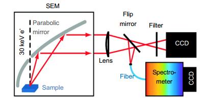
Figure 1.
Schematic overview of a CL imaging spectrometer with spectral analysis function.
-
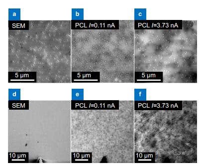
Figure 2.
(a) SEM image of the GaN/InGaN multiple quantum well surface. (b, c) CL image of the same area of (a) at electron beam currents of 0.11 nA and 3.73 nA, respectively. (d–f) The same images at lower magnification clearly demonstrate the decline in luminous efficiency.
-
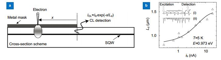
Figure 3.
(a) Schematic of CL method for the measurement of Ld. (b) Ld as a function of the electron-beam current ib at 5 K. Inset: Schematic of the carrier transport in conjunction with localized states for low (ⅰ) and high (ⅱ) densities of localized states.
-
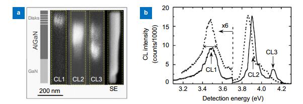
Figure 4.
(a) Schematic, CL images and SEM image of the single nanocolumn. (b) CL spectra of two single GaN/AlGaN nanocolumns.
-
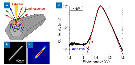
Figure 5.
(a) Schematic of the electron beam interaction with nanowire and luminescence emission. (b) SEM image of a single nanowire. (c) CL image of a single GaAs nanowire measured at 30 K. (d) CL spectrum from nanowire at room temperature and the fit (red curve).
-
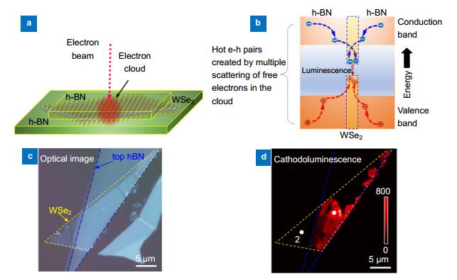
Figure 6.
(a) Schematic of hBN/WSe2/hBN van der waals heterojunction excited by electron beam. (b) Process of the generation, diffusion, and recombination of electron−hole (e-h) pairs in heterojunction. (c) Optical microscope image of a hBN/ WSe2/hBN heterostructure. (d) Monochromatic CL image of the heterostructure at WSe2 emission energy (1.66 eV).
-
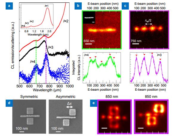
Figure 7.
(a) FDTD (red) simulated, dark-field (black) scattering and CL emission spectrum of Au antenna indicate the standing wave eigenmodes. CL images of nanoantenna with bandpass filter at (b) 650 nm and (c) 750 nm. Integrated CL intensity shows the standing wave plasmon resonances. (d) SEM images of symmetric and asymmetric coupling structure of nanowire and nanoantennas. (e) CL images of two coupling structures with bandpass filter at 850 nm.
-
Figure 8.
(a) Schematic of the electron stimulated heptamer nanostructure. (b) Left: panchromatic CL image of Au heptamer nanostructures. Right: part of SEM image of Au heptamer. (c) CL spectra measured from impinging positions as indicated in (b).
-
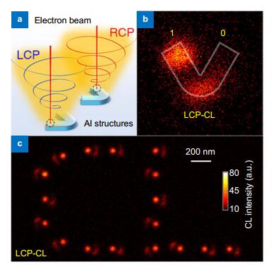
Figure 9.
(a) Schematic of circular polarization resolved Al nanoantenna with electron beam excitation. (b) LCP CL image of a single nanostructure with a bandpass of 657 nm. (c) LCP CL image for the helicity-dependent 2D display of capital letters "CL".
-
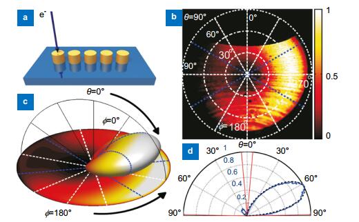
Figure 10.
(a) Schematic of the excitation geometry. (b) CL emission intensity as a function of angle. (c) 3D representation of theoretical radiation pattern for this excitation position and wavelength, together with a projection onto a 2D grid. (d) Cross-cut through the angular data showing CL intensity as a function of θ (blue curve) together with theory (black dashed curve).
-
Figure 11.
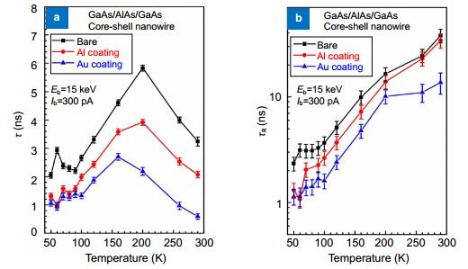
Measured carrier decay times τ(T) in (a) and radiative lifetime τR(T) in (b) with time-resolved CL spectroscopy.


