
 E-mail Alert
 RSS
RSS
| Citation: |
Zhang Yuhu, Xu Haitao, Li Yawen, et al. The improvement of TFT lithography plane compensation[J]. Opto-Electronic Engineering, 2019, 46(5): 180444. doi: 10.12086/oee.2019.180444

|
The improvement of TFT lithography plane compensation
-
Abstract
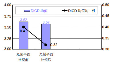
When the line width or line space of thin film transistor (TFT) is close to the resolution of the lithography machine, it is easy to appear the defect of photoresist remain in lithography pattern. In order to improve this problem, based on the position of the best lithography pattern, the optimal compensation amount of lithography plane of the lithography machine is calculated, so lithography plane is improved. Firstly, by the compensation of the lithography plane, the flatness of the plate stage and the focal plane, the value of the plate surface height is calculated in the lithography region. Then, according to the lithography pattern in the lithography region, the optimum position of the lithography region is found, and take this location as the zero point, the relative height difference between the total lithography region and the optimum position is calculated. Secondly, the fitting plane of the height difference in the lithography region is done, and the compensation is calculated when the fitting plane is the horizontal plane that is perpendicular to the Z axis, which is the optimal compensation of the lithography plane in the lithography region. Finally, the compensation is used to compensate the lithography plane, so that the lithography plane in the lithography region tends to the same optimal lithography plane. The results show that the lithography pattern can be clearly formed in the lithography region after the lithography plane is offset, the defect of the photoresist remain is improved, at the same time, the average value of the develop inspection critical dimension (DICD) is reduced by 1.38% in the target value range, and the uniformity of the DICD is increased by 20%.-
Keywords:
- thin film transistor /
- lithography plane /
- optimal compensation /
- plane fitting
-

-
References
[1] 王新久.液晶光学和液晶显示[M].北京:科学出版社, 2006: 230-251. Wang X J. Liquid Crystal Optics & Liquid Cristal Display[M]. Beijing: Science Press, 2006: 230-251. [2] 邵喜斌.液晶显示技术的最新进展[J].液晶与显示, 2000, 15(3): 163-170. doi: 10.3969/j.issn.1007-2780.2000.03.001 Shao X B. Recent progress of liquid crystal display technology[J]. Chinese Journal of Liquid Crystals and Displays, 2000, 15(3): 163-170. doi: 10.3969/j.issn.1007-2780.2000.03.001 [3] 车春城.广视角FFS技术CELL研究与设计[D].成都: 电子科技大学, 2007: 1-6. Che C C. CELL research and design of FFS wide viewing angle technology[D]. Chengdu: University of Electronic Science and Technology of China, 2007: 1-6. CNKI:CDMD:2.2007.100479 [4] 童林夙. 2012年后的平板显示世界[J].现代显示, 2007(7): 6-16. doi: 10.3969/j.issn.1006-6268.2007.07.002 Tong L S. Flat panel displays after 2012[J]. Advanced Display, 2007(7): 6-16. doi: 10.3969/j.issn.1006-6268.2007.07.002 [5] 黎午升, 惠官宝, 崔承镇, 等.在镜像投影曝光机上使用相移掩膜提高解像力的初步研究[J].液晶与显示, 2014, 29(4): 544-547. Li W S, Hui G B, Cui C Z, et al. Preliminary study on improving resolution on mirror projection mask aligner with phase shift mask[J]. Chinese Journal of Liquid Crystals and Displays, 2014, 29(4): 544-547. [6] 肖文俊.薄膜晶体管液晶显示器的串扰研究[D].北京: 北京交通大学, 2014: 1-4. Xiao W J. A Research on crosstalk in TFT-LCDs[D]. Beijing: Beijing Jiaotong University, 2014: 1-4. [7] Chun J Y, Kang C H, Ahn S J, et al. A-Si TFT-LCD mobile display with high pixel density using PenTile RGB WTM algorithm[J]. Chinese Journal of Liquid Crystals and Displays, 2006, 21(5): 474-477. [8] 冯伯儒, 张锦, 侯德胜, 等.相移掩模和光学邻近效应校正光刻技术[J].光电工程, 2001, 28(1): 1-5. doi: 10.3969/j.issn.1003-501X.2001.01.001 Feng B R, Zhang J, Hou D S, et al. Optical microlithography with phase-shifting mask and optical proximity effect correction[J]. Opto-Electronic Engineering, 2001, 28(1): 1-5. doi: 10.3969/j.issn.1003-501X.2001.01.001 [9] 缪小运.先进光刻系统中焦平面测量与控制的研究[D].上海: 复旦大学, 2006: 5-9. Miu X Y. Focal Plane Measure and Control Study[D]. Shanghai: Fudan University, 2006: 5-9. 10.7666/d.y1021731 [10] 黎午升, 惠官宝, 崔承镇, 等.相移掩膜应用于显示技术光刻细线化的初步研究[J].光电子技术, 2014, 34(4): 234-237. doi: 10.3969/j.issn.1005-488X.2014.04.005 Li W S, Hui G B, Cui C Z, et al. Preliminary study on improving photolithographic resolution of display technology with phase shift mask[J]. Optoelectronic Technology, 2014, 34(4): 234-237. doi: 10.3969/j.issn.1005-488X.2014.04.005 -
Overview

Overview: The traditional method of the thin film transistor (TFT) lithography plane compensation is realized by ensuring the flatness of photoresist plane and the photoresist plane is on the focal plane of the lithography machine, which is achieved by the compensation of flatness of the plate stage and the focus compensation of lithography machine. However, due to the existence of the compensation error, the quality of the actual lithography product picture is different from the ideal situation, when the TFT line width or line space is close to the minimum resolution of the lithography machine. The difference will lead to the defect of remaining photoresist, which seriously affects the yield of the lithography products. In order to solve the problem, based on the position of the best lithography pattern, the optimal compensation amount of lithography plane of the lithography machine is calculated. The difference of the result between the actual lithography product and the compensation of the lithography plane is reduced by the optimal compensation, which is compensated for the lithography machine. So, lithography plane is improved. Firstly, by the compensation of the lithography plane, the flatness of the plate stage and the focal plane, the value of the plate surface height is calculated in the lithography region. Then, according to the lithography pattern in the lithography region, the optimum position of the lithography region is found. Taking this location as the zero point, the relative height difference between the total lithography region and the optimum position is calculated. Secondly, the fitting plane of the height difference in the lithography region is done, and the compensation is calculated when the fitting plane is the horizontal plane that is perpendicular to the Z axis, which is the optimal compensation of the lithography plane in the lithography region. Finally, the compensation is used to compensate the lithography plane, so that the lithography plane in the lithography region tends to the same optimal lithography plane. The results show that, compared with no compensation, the lithography pattern can be clearly formed in the lithography region after the lithography plane is offset. The defect of the remaining photoresist is improved. At the same time, the average value of the DICD is reduced by 1.38% in the target value range, the uniformity of the DICD is increased by 20%, and the ability of small line lithography for the lithography machine at the minimum resolution has been significantly improved.
-
Access History
Figures(13)
Tables(6)
Article Metrics


Export File
Citation
Zhang Yuhu, Xu Haitao, Li Yawen, et al. The improvement of TFT lithography plane compensation[J]. Opto-Electronic Engineering, 2019, 46(5): 180444. doi: 10.12086/oee.2019.180444
Format
Content
 DownLoad:


-
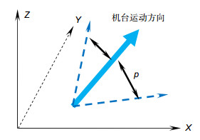
Figure 1.
The picture of pitching
-
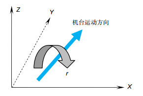
Figure 2.
The picture of rolling
-
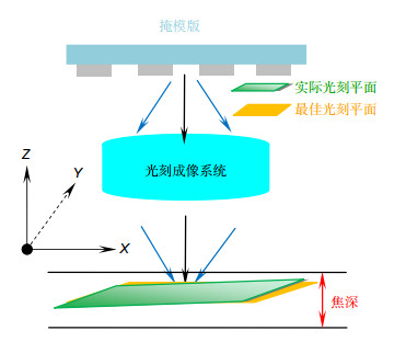
Figure 3.
The process of lithography offset
-
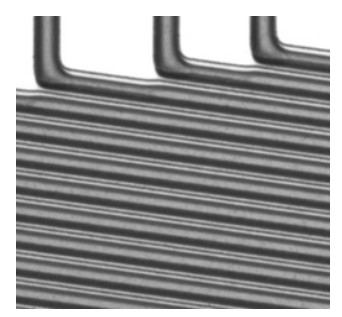
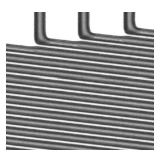
Figure 4.
The pattern picture of PR remain
-
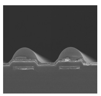
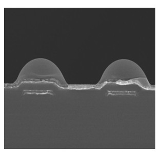
Figure 5.
The SEM picture of PR remain
-
Figure 6.
The picture of lithography plane before compensation
-
Figure 7.
The picture of lithography plane after compensation
-
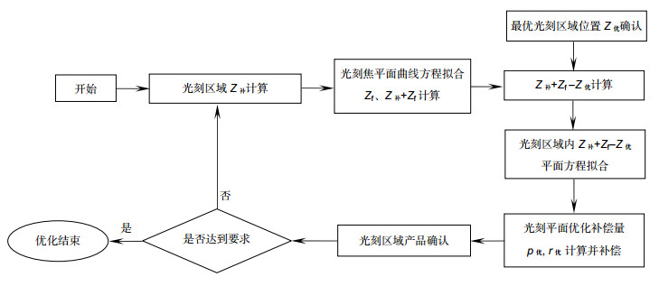
Figure 8.
The diagram of improvement process
-
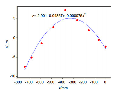
Figure 9.
The fitting equation of focus curve
-
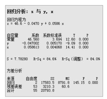
Figure 10.
The fitting plane equation of regression
-
Figure 11.
The pattern picture of PR remain in high incidence area after improvemen
-
Figure 12.
The SEM picture of PR remain in high incidence area after improvement
-
Figure 13.
The DICD result of the offse


