
 E-mail Alert
 RSS
RSS
| Citation: |
Hou Shuang, Liu Qing, Xing Zhiyang, et al. Effects of Sn doping on Ga2O3-based solar blind photodetectors[J]. Opto-Electronic Engineering, 2019, 46(10): 190011. doi: 10.12086/oee.2019.190011

|
Effects of Sn doping on Ga2O3-based solar blind photodetectors
-
Abstract
In order to improve the performance of Ga2O3-based photodetectors (PDs), Sn-doped gallium oxide thin films were prepared on sapphire substrates by molecular beam epitaxy system. The influence of Sn doping on both Ga2O3 crystal structure and photoelectric properties of metal-semiconductor-metal (MSM) PDs were investigated. X-ray diffraction shows that gallium oxide films change from single crystal to polycrystalline phase when increasing the growth temperature of SnO2. When 254 nm and 42 μW/cm2 light was used, the responsivity of Sn-doped Ga2O3 photodetectors reached 444.51 A/W. Compared with the undoped β-Ga2O3 PDs, the photocurrent and responsivity of Sn-doped PDs were almost increased by two orders of magnitude, suggesting the improvement on PD performance. Spectral response shows that the cut-off wavelength of Sn-doped PDs changes from 252 nm to 274 nm by increasing Sn dose, which reveals an efficient way toward the development of the UV PDs focus on longer wavelengths. However, Sn doping also introduces impurity levels, resulting in poor time response of the MSM PDs.-
Keywords:
- Sn doping /
- β-Ga2O3 /
- solar blind ultraviolet photodetector /
- responsivity
-

-
References
[1] 王保华, 李妥妥, 郑国宪.日盲紫外探测系统研究[J].激光与光电子学进展, 2014, 51(2): 022202. doi: 10.3788/LOP51.022202 Wang B H, Li T T, Zheng G X. Research of solar blind ultraviolet detection system[J]. Laser & Optoelectronics Progress, 2014, 51(2): 022202. doi: 10.3788/LOP51.022202 [2] Giza R H, Acevedo P A, Bliss J D. Ultraviolet scene simulation for missile approach warning system testing[J]. Proceedings of SPIE, 1997, 3084: 282–291. doi: 10.1117/12.280958 [3] Brown D M, Downey E, Kretchmer J, et al. SiC flame sensors for gas turbine control systems[J]. Solid-State Electronics, 1998, 42(5): 755–760. doi: 10.1016/S0038-1101(97)00260-8 [4] Sang L W, Liao M Y, Sumiya M. A comprehensive review of semiconductor ultraviolet photodetectors: from thin film to one-dimensional nanostructures[J]. Sensors, 2013, 13(8): 10482–10518. doi: 10.3390/s130810482 [5] Razeghi M. Short-wavelength solar-blind detectors-status, prospects, and markets[J]. Proceedings of the IEEE, 2002, 90(6): 1006–1014. doi: 10.1109/JPROC.2002.1021565 [6] Dong K X, Chen D J, Zhang Y Y, et al. AlGaN solar-blind APD with low breakdown voltage[J]. Opto-Electronic Engineering, 2017, 44(4): 405–409. doi: 10.3969/j.issn.1003-501X.2017.04.004 [7] Qian L X, Wu Z H, Zhang Y Y, et al. Ultrahigh-responsivity, rapid-recovery, solar-blind photodetector based on highly nonstoichiometric amorphous gallium oxide[J]. ACS Photonics, 2017, 4(9): 2203–2211. doi: 10.1021/acsphotonics.7b00359 [8] Guo D Y, Liu H, Li P G, et al. Zero-power-consumption solar-blind photodetector based on β‑Ga2O3/NSTO heterojunction[J]. ACS Applied Materials & Interfaces, 2017, 9(2): 1619–1628. doi: 10.1021/acsami.6b13771 [9] Qian L X, Zhang H F, Lai P T, et al. High-sensitivity β-Ga2O3 solar-blind photodetector on high-temperature pretreated c-plane sapphire substrate[J]. Optical Materials Express, 2017, 7(10): 3643–3653. doi: 10.1364/OME.7.003643 [10] Oh S, Jung Y, Mastro M A, et al. Development of solar-blind photodetectors based on Si-implanted β-Ga2O3[J]. Optics Express, 2015, 23(22): 28300–28305. doi: 10.1364/OE.23.028300 [11] Ravadgar P, Horng R H, Yao S D, et al. Effects of crystallinity and point defects on optoelectronic applications of β-Ga2O3 epilayers[J]. Optics Express, 2013, 21(21): 24599–24610. doi: 10.1364/OE.21.024599 [12] 石雄林, 刘宏宇, 侯爽, 等.表面等离子体在氧化镓基紫外探测器中的应用[J].光电工程, 2018, 45(2): 170728. doi: 10.12086/oee.2018.170728 Shi X L, Liu H Y, Hou S, et al. The applications of surface plasmons in Ga2O3 ultraviolet photodetector[J]. Opto-Electronic Engineering, 2018, 45(2): 170728. doi: 10.12086/oee.2018.170728 [13] Ueda N, Hosono H, Waseda R, et al. Synthesis and control of conductivity of ultraviolet transmitting β-Ga2O3 single crystals[J]. Applied Physics Letters, 1997, 70(26): 3561–3563. doi: 10.1063/1.119233 [14] Matsumoto T, Aoki M, Kinoshita A, et al. Absorption and reflection of vapor grown single crystal platelets of β-Ga2O3[J]. Japanese Journal of Applied Physics, 1974, 13(10): 1578. doi: 10.1143/JJAP.13.1578 [15] Kohei Sasaki, Akito Kuramata, Takekazu Masui, et al. Device-Quality β-Ga2O3 Epitaxial Films Fabricated by Ozone Molecular Beam Epitaxy[J]. Applied Physics Express, 2012, 5, 035502. doi: 10.1143/APEX.5.035502 [16] Chang P C, Fan Z Y, Tseng W Y, et al. β-Ga2O3 nanowires: synthesis, characterization, and p-channel field-effect transistor[J]. Applied Physics Letters, 2005, 87(22): 222102. doi: 10.1063/1.2135867 [17] Varley J B, Weber J R, Janotti A, et al. Oxygen vacancies and donor impurities in β-Ga2O3[J]. Applied Physics Letters, 2010, 97(14): 142106. doi: 10.1063/1.3499306 [18] Orita M, Hiramatsu H, Ohta H, et al. Preparation of highly conductive, deep ultraviolet transparent β-Ga2O3 thin film at low deposition temperatures[J]. Thin Solid Films, 2002, 411(1): 134–139. doi: 10.1016/S0040-6090(02)00202-X [19] Du X J, Li Z, Luan C N, et al. Preparation and characterization of Sn-doped β-Ga2O3 homoepitaxial films by MOCVD[J]. Journal of Materials Science, 2015, 50(8): 3252–3257. doi: 10.1007/s10853-015-8893-4 [20] Usui Y, Nakauchi D, Kawano N, et al. Scintillation and optical properties of Sn-doped Ga2O3 single crystals[J]. Journal of Physics and Chemistry of Solids, 2018, 117: 36–41. doi: 10.1016/j.jpcs.2018.02.027 [21] Sasaki K, Higashiwaki M, Kuramata A, et al. Growth temperature dependences of structural and electrical properties of Ga2O3 epitaxial films grown on β-Ga2O3 (010) substrates by molecular beam epitaxy[J]. Journal of Crystal Growth, 2014, 392: 30–33. doi: 10.1016/j.jcrysgro.2014.02.002 [22] Li M Q, Yang N, Wang G G, et al. Highly preferred orientation of Ga2O3 films sputtered on SiC substrates for deep UV photodetector application[J]. Applied Surface Science, 2019, 471: 694–702. doi: 10.1016/j.apsusc.2018.12.045 [23] Carrano J C, Li T, Grudowski P A, et al. Comprehensive characterization of metal-semiconductor-metal ultraviolet photodetectors fabricated on single-crystal GaN[J]. Journal of Applied Physics, 1998, 83(11): 6148–6160. doi: 10.1063/1.367484 [24] Guo D Y, Wu Z P, Li P G, et al. Fabrication of β-Ga2O3 thin films and solar-blind photodetectors by laser MBE technology[J]. Optical Materials Express, 2014, 4(5): 1067–1076. doi: 10.1364/OME.4.001067 -
Overview

Overview: Deep ultraviolet (DUV) photodetectors with solar-blind sensitivity (cutoff wavelength shorter than 280 nm) have received much attention because their photo response can be further restricted within the DUV region only even under sun or room illuminations. Solar-blind DUV photodetectors (PDs) are important devices that can be used in various commercial and military applications, such as flame detector, missile plume sensor, and ozone holes' monitor. Currently, Si-based photodiodes are the most commonly used ultraviolet photodetector in the commercial market because of their high compatibility with the highly mature silicon processes. However, expensive and cumbersome Wood's optical filters are required because Si is sensitive to infrared, visible, and near UV lights due to its small bandgap (1.1 eV~1.3 eV). Therefore, PDs based on wide-bandgap (Eg) semiconductors are regarded as more promising alternatives. In recent years, several wide bandgap materials consisting of AlGaN, Ga2O3, ZnMgO, BN, and diamond were proposed for solar-blind DUV photodetectors. Among these materials, gallium oxide, which has an Eg of 4.9 eV, is intrinsically suitable for solar-blind photodetection. In the past few years, gallium oxide-based metal-semiconductor-metal (MSM) PDs have been intensively explored.
It is found that the undoped Ga2O3 thin films are of n-type conductivity as defects such as oxygen vacancies will be introduced during the preparation process. However, pure β-Ga2O3 demonstrates poor conductivity at room temperature because of low electronic mobility, hindering its practical applications based on conductance response. In order to overcome this obstacle, intentionally controlled doping becomes a very important and feasible method. Tetravalent Sn is a superb doping candidate for Ga2O3 because it is not only an effective n-type dopant, but also has a close ionic radius with the octahedrally coordinated Ga3+. Masahiro Orita group used the method of pulsed laser deposition (PLD) to grow Sn-doped Ga2O3 film in 2002; Azuaki Akaiwa prepared a Sn-doped Ga2O3 film in 2012 using the spray-assisted mist chemical vapor deposition (mist CVD) method. In 2014, Du Xuejian and others from Shandong University of China used the metal-organic chemical vapor deposition (MOCVD) method to prepare a low-resistivity Sn-doped gallium oxide homoepitaxial film. However, there are few reports on the Sn-doped gallium oxide thin films preparation of molecular beam epitaxy (MBE), which is a new and widely used film preparation technology developed with the improvement of semiconductor crystal quality requirements. In this work, we explored the growth of Sn doped Ga2O3 film on sapphire substrates by MBE method. Solar-blind photodetectors with MSM structure based on Sn doped Ga2O3 thin films were fabricated and compared with the undoped PDs. Result shows that photocurrent and responsivity almost increased by two order of magnitude for Sn doped devices, suggesting devices performance of PD can be improved by doping Sn in Ga2O3 films.
-
Access History

Export File
Citation
Hou Shuang, Liu Qing, Xing Zhiyang, et al. Effects of Sn doping on Ga2O3-based solar blind photodetectors[J]. Opto-Electronic Engineering, 2019, 46(10): 190011. doi: 10.12086/oee.2019.190011
Format
Content
 DownLoad:
-
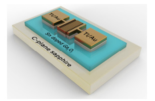
Figure 1.
The schematic diagram of the Ga2O3 MSM solar-blind ultraviolet PD
-
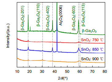
Figure 2.
XRD spectra of β-Ga2O3 and Sn doped β-Ga2O3 films deposited at different SnO2 temperatures
-
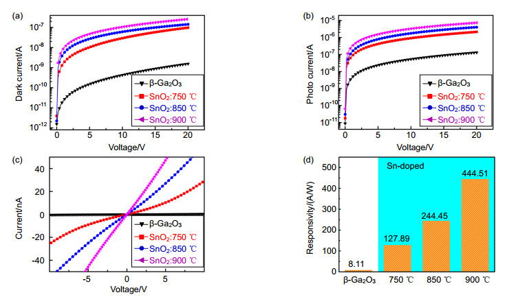
Figure 3.
The current-voltage (I-V) of the Ga2O3 MSM PDs with different SnO2 temperatures. (a) Idark−V characteristics on asemilogarithmic scale; (b) I−V characteristics under 254 nm DUV illumination on a semilogarithmic scale; (c) Idark−V characteristics on a linear scale; (d) Responsivity of Sn-doped Ga2O3 MSM PDs with different SnO2 temperatures
-
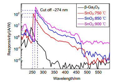
Figure 4.
Spectral response of the Ga2O3 MSM PDs on a semilogarithmic scale
-
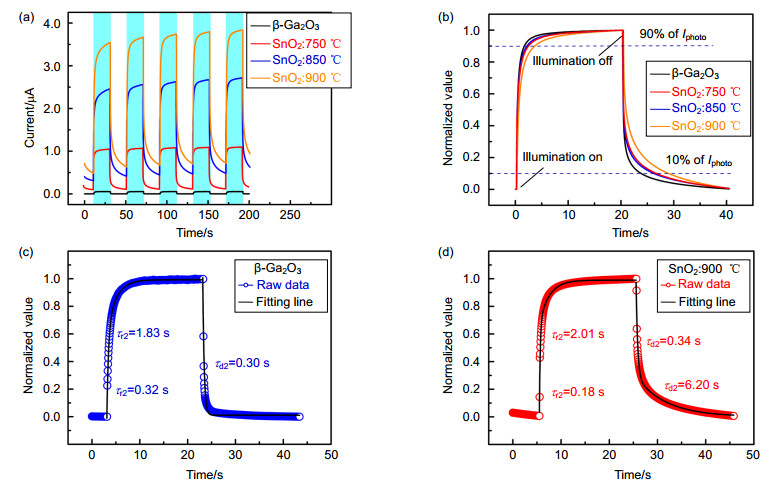
Figure 5.
Time-dependent photoresponse of the Ga2O3 MSM PDs with different SnO2 temperature. (a) Response for multicycles on a linear scale; (b) Normalized transient response on a linear scale; (c) Experimental and fitted curves of rise and decay processes for β-Ga2O3 PDs; (d) Sn doped β-Ga2O3 PDs with SnO2 temperature of 900 ℃


