
 E-mail Alert
 RSS
RSS
| Citation: |
Yatsui T. Recent improvement of silicon absorption in opto-electric devices. Opto-Electron Adv 2, 190023 (2019). doi: 10.29026/oea.2019.190023

|
Review Open Access
Recent improvement of silicon absorption in opto-electric devices
-
Abstract
Silicon dominates the contemporary electronic industry. However, being an indirect band-gap material, it is a poor absorber of light, which decreases the efficiency of Si-based photodetectors and photovoltaic devices. This review highlights recent studies performed towards improving the optical absorption of Si. A summary of recent theoretical approaches based on the first principle calculation has been provided. It is followed by an overview of recent experimental approaches including scattering, plasmon, hot electron, and near-field effects. The article concludes with a perspective on the future research direction of Si-based photodetectors and photovoltaic devices.-
Keywords:
- Si /
- indirect band gap /
- plasmon /
- first principle calculation /
- near-field effect
-

-
References
[1] Green M A, Emery K, Hishikawa Y, Warta W, Dunlop E D. Solar cell efficiency tables (Version 45). Prog Photovoltaics: Res Appl 23, 1-9 (2015). doi: 10.1002/pip.2573 [2] Battaglia C, Cuevas A, De Wolf S. High-efficiency crystalline silicon solar cells: status and perspectives. Energy Environ Sci 9, 1552-1576 (2016). doi: 10.1039/C5EE03380B [3] Yatsui T, Okada S, Takemori T, Sato T, Saichi K et al. Enhanced photo-sensitivity in a Si photodetector using a near-field assisted excitation. Commun Phys 2, 62 (2019). doi: 10.1038/s42005-019-0173-1 [4] Soref R. The past, present, and future of silicon photonics. IEEE J Sel Top Quantum Electron 12, 1678-1687 (2006). doi: 10.1109/JSTQE.2006.883151 [5] Asghari M, Krishnamoorthy A V. Energy-efficient communication. Nat Photonics 5, 268-270 (2011). doi: 10.1038/nphoton.2011.68 [6] Wirths S, Geiger R, von den Driesch N, Mussler G, Stoica T et al. Lasing in direct-bandgap GeSn alloy grown on Si. Nat Photonics 9, 88-92 (2015). doi: 10.1038/nphoton.2014.321 [7] Romagnoli M, Sorianello V, Midrio M, Koppens F H L, Huyghebaert C et al. Graphene-based integrated photonics for next-generation datacom and telecom. Nat Rev Mater 3, 392-414 (2018). doi: 10.1038/s41578-018-0040-9 [8] Kirkengen M, Bergli J, Galperin Y M. Direct generation of charge carriers in c-Si solar cells due to embedded nanoparticles. J Appl Phys 102, 093713 (2007). doi: 10.1063/1.2809368 [9] Jung J, Trolle M L, Pedersen K, Pedersen T G. Indirect near-field absorption mediated by localized surface plasmons. Phys Rev B 84, 165447 (2011). doi: 10.1103/PhysRevB.84.165447 [10] Yamaguchi M, Nobusada K. Indirect interband transition induced by optical near fields with large wave numbers. Phys Rev B 93, 195111 (2016). doi: 10.1103/PhysRevB.93.195111 [11] Martin R M. Electronic Structure: Basic Theory and Practical Methods (Cambridge University Press, Cambridge, 2004). [12] Ashcroft N W, Mermin N D. Solid State Physics (Hold, Rinehart, and Winston, New York, 1976). [13] Jackson J D. Classical Electrodynamics (Wiley, New York, 1962). [14] Noda M, Iida K, Yamaguchi M, Yatsui T, Nobusada K. Direct wave-vector excitation in an indirect-band-gap semiconductor of silicon with an optical near-field. Phys Rev Appl 11, 044053 (2019). doi: 10.1103/PhysRevApplied.11.044053 [15] Noda M, Ishimura K, Nobusada K, Yabana K, Boku T. Massively-parallel electron dynamics calculations in real-time and real-space: Toward applications to nanostructures of more than ten-nanometers in size. J Comput Phys 265, 145-155 (2014). doi: 10.1016/j.jcp.2014.02.006 [16] Noda M, Yamaguchi M, Nobusada K. Second harmonic excitation of acetylene by the optical near field generated in a porous material. J Phys Chem C 121, 11687-11692 (2017). doi: 10.1021/acs.jpcc.7b02744 [17] Iida K, Noda M, Nobusada K. Development of theoretical approach for describing electronic properties of hetero-interface systems under applied bias voltage. J Chem Phys 146, 084706 (2017). doi: 10.1063/1.4976970 [18] Baker-Finch S C, McIntosh K R. Reflection distributions of textured monocrystalline silicon: implications for silicon solar cells. Prog Photovoltaics: Res Appl 21, 960-971 (2013). doi: 10.1002/pip.2186 [19] Peng K Q, Xu Y, Wu Y, Yan Y J, Lee S T et al. Aligned single-crystalline si nanowire arrays for photovoltaic applications. Small 1, 1062-1067 (2005). doi: 10.1002/smll.200500137 [20] Shen M Y, Crouch C H, Carey J E, Mazur E. Femtosecond laser-induced formation of submicrometer spikes on silicon in water. Appl Phys Lett 85, 5694-5696 (2004). doi: 10.1063/1.1828575 [21] Sarnet T, Carey J E, Mazur E. From black silicon to photovoltaic cells, using short pulse lasers. AIP Conf Proc 1464, 219-228 (2012). [22] Savin H, Repo P, von Gastrow G, Ortega P, Calle E et al. Black silicon solar cells with interdigitated back-contacts achieve 22.1% efficiency. Nat Nanotechnol 10, 624-628 (2015). doi: 10.1038/nnano.2015.89 [23] Schaadt D M, Feng B, Yu E T. Enhanced semiconductor optical absorption via surface plasmon excitation in metal nanoparticles. Appl Phys Lett 86, 063106 (2005). doi: 10.1063/1.1855423 [24] Nakayama K, Tanabe K, Atwater H A. Plasmonic nanoparticle enhanced light absorption in GaAs solar cells. Appl Phys Lett 93, 121904 (2008). doi: 10.1063/1.2988288 [25] Bohren C F, Huffman D R. Absorption and Scattering of Light by Small Particles (Wiley, New York, 1998). [26] Stuart H R, Hall D G. Absorption enhancement in silicon-on-insulator waveguides using metal island films. Appl Phys Lett 69, 2327-2329 (1996). doi: 10.1063/1.117513 [27] Pillai S, Catchpole K R, Trupke T, Green M A. Surface plasmon enhanced silicon solar cells. J Appl Phys 101, 093105 (2007). doi: 10.1063/1.2734885 [28] Catchpole K R, Polman A. Design principles for particle plasmon enhanced solar cells. Appl Phys Lett 93, 191113 (2008). doi: 10.1063/1.3021072 [29] Catchpole K R, Polman A. Plasmonic solar cells. Opt Express 16, 21793-21800 (2008). doi: 10.1364/OE.16.021793 [30] Kelzenberg M D, Boettcher S W, Petykiewicz J A, Turner-Evans D B, Putnam M C et al. Enhanced absorption and carrier collection in Si wire arrays for photovoltaic applications. Nat Mater 9, 239-244 (2010). doi: 10.1038/nmat2635 [31] Kelzenberg M D, Turner-Evans D B, Putnam M C, Boettcher S W, Briggs R M et al. High-performance Si microwire photovoltaics. Energy Environ Sci 4, 866-871 (2011). doi: 10.1039/c0ee00549e [32] Grand J, Adam P M, Grimault A S, Vial A, de la Chapelle M L et al. Optical extinction spectroscopy of oblate, prolate and ellipsoid shaped gold nanoparticles: experiments and theory. Plasmonics 1, 135-140 (2006). doi: 10.1007/s11468-006-9014-7 [33] Wei Q H, Su K H, Durant S, Zhang X. Plasmon resonance of finite one-dimensional Au nanoparticle chains. Nano Lett 4, 1067-1071 (2004). doi: 10.1021/nl049604h [34] Fan P Y, Chettiar U K, Cao L Y, Afshinmanesh F, Engheta N et al. An invisible metal-semiconductor photodetector. Nat Photonics 6, 380-385 (2012). doi: 10.1038/nphoton.2012.108 [35] Wang Y, Sun T Y, Paudel T, Zhang Y, Ren Z F et al. Metamaterial-plasmonic absorber structure for high efficiency amorphous silicon solar cells. Nano Lett 12, 440-445 (2012). doi: 10.1021/nl203763k [36] Esfandyarpour M, Garnett E C, Cui Y, McGehee M D, Brongersma M L. Metamaterial mirrors in optoelectronic devices. Nat Nanotechnol 9, 542-547 (2014). doi: 10.1038/nnano.2014.117 [37] Yatsui T, Nomura W, Ohtsu M. Self-assembly of size- and position-controlled ultralong nanodot chains using near-field optical desorption. Nano Lett 5, 2548-2551 (2005). doi: 10.1021/nl051898z [38] Yukutake S, Kawazoe T, Yatsui T, Nomura W, Kitamura K et al. Selective photocurrent generation in the transparent wavelength range of a semiconductor photovoltaic device using a phonon-assisted optical near-field process. Appl Phys B 99, 415-422 (2010). doi: 10.1007/s00340-010-3999-5 [39] Naik G V, Shalaev V M, Boltasseva A. alternative plasmonic materials: beyond gold and silver. Adv Mater 25, 3264-3294 (2013). doi: 10.1002/adma.201205076 [40] Matsui H, Badalawa W, Hasebe T, Furuta S, Nomura W et al. Coupling of Er light emissions to plasmon modes on In2O3: Sn nanoparticle sheets in the near-infrared range. Appl Phys Lett 105, 041903 (2014). doi: 10.1063/1.4892004 [41] Goykhman I, Desiatov B, Khurgin J, Shappir J, Levy U. Locally oxidized silicon surface-plasmon schottky detector for telecom regime. Nano Lett 11, 2219-2224 (2011). doi: 10.1021/nl200187v [42] Knight M W, Sobhani H, Nordlander P, Halas N J. Photodetection with active optical antennas. Science 332, 702-704 (2011). doi: 10.1126/science.1203056 [43] Sobhani A, Knight M W, Wang Y M, Zheng B, King N S et al. Narrowband photodetection in the near-infrared with a plasmon-induced hot electron device. Nat Commun 4, 1643 (2013). doi: 10.1038/ncomms2642 [44] Ho Y L, Huang L C, Delaunay J J. Spectrally selective photocapacitance modulation in plasmonic nanochannels for infrared imaging. Nano Lett 16, 3094-3100 (2016). doi: 10.1021/acs.nanolett.6b00326 [45] Pankove J I. Optical Processes in Semiconductors (Dover, New York, 1971). [46] Loferski J J. Theoretical considerations governing the choice of the optimum semiconductor for photovoltaic solar energy conversion. J Appl Phys 27, 777-784 (1956). doi: 10.1063/1.1722483 [47] Taflove A, Hagness S C. Computational Electrodynamics: The Finite-Difference Time-Domain Method 3rd ed (Artech House, London, 2005). [48] Richard S, Aniel F, Fishman G. Energy-band structure of Ge, Si, and GaAs: A thirty-band k∙p method. Phys Rev B 70, 235204 (2004). doi: 10.1103/PhysRevB.70.235204 [49] Maier S A. Plasmonics: Fundamentals and Applications (Springer, New York, 2007). [50] Koshida N, Koyama H. Visible electroluminescence from porous silicon. Appl Phys Lett 60, 347-349 (1992). doi: 10.1063/1.106652 [51] Zheng J P, Jiao K L, Shen W P, Anderson W A, Kwok H S. Highly sensitive photodetector using porous silicon. Appl Phys Lett 61, 459-461 (1992). doi: 10.1063/1.107884 [52] Yatsui T, Ohtsu M. Production of size-controlled Si nanocrystals using self-organized optical near-field chemical etching. Appl Phys Lett 95, 043104 (2009). doi: 10.1063/1.3193536 [53] Yatsui T, Nakahira Y, Nakamura Y, Morimoto T, Kato Y et al. Realization of red shift of absorption spectra using optical near-field effect. Nanotechnology 30, 34LT02 (2019). doi: 10.1088/1361-6528/ab2092 [54] Iwasa T, Nobusada K. Nonuniform light-matter interaction theory for near-field-induced electron dynamics. Phys Rev A 80, 043409 (2009). doi: 10.1103/PhysRevA.80.043409 [55] Yamaguchi M, Nobusada K, Kawazoe T, Yatsui T. Two-photon absorption induced by electric field gradient of optical near-field and its application to photolithography. Appl Phys Lett 106, 191103 (2015). doi: 10.1063/1.4921005 [56] Yamaguchi M, Nobusada K, Yatsui T. Nonlinear optical response induced by a second-harmonic electric-field component concomitant with optical near-field excitation. Phys Rev A 92, 043809 (2015). doi: 10.1103/PhysRevA.92.043809 [57] Yamaguchi M, Nobusada K. Large hyperpolarizabilities of the second harmonic generation induced by nonuniform optical near fields. J Phys Chem C 120, 23748-23755 (2016). doi: 10.1021/acs.jpcc.6b08507 [58] Fang C Z, Liu Y, Zhang Q F, Han G Q, Gao X et al. Germanium-tin alloys: applications for optoelectronics in mid-infrared spectra. Opto-Electron Adv 1, 180004 (2018). doi: 10.29026/oea.2018.180004 [59] Lei S D, Ge L H, Najmaei S, George A, Kappera R et al. Evolution of the electronic band structure and efficient photo-detection in atomic layers of InSe. ACS Nano 8, 1263-1272 (2014). doi: 10.1021/nn405036u [60] Li H, Han X, Pan D, Yan X, Wang H W et al. Bandgap engineering of inse single crystals through S substitution. Cryst Growth Des 18, 2899-2904 (2018). doi: 10.1021/acs.cgd.7b01751 [61] Hamer M J, Zultak J, Tyurnina A V, Zólyomi V, Terry D et al. Indirect to direct gap crossover in two-dimensional InSe revealed by angle-resolved photoemission spectroscopy. ACS Nano 13, 2136-2142 (2019). [62] Wang X D, Wang P, Wang J L, Hu W D, Zhou X H et al. Ultrasensitive and broadband MoS2 photodetector driven by ferroelectrics. Adv Mater 27, 6575-6581 (2015). doi: 10.1002/adma.201503340 [63] Kufer D, Konstantatos G. Highly sensitive, encapsulated MoS2 photodetector with gate controllable gain and speed. Nano Lett 15, 7307-7313 (2015). doi: 10.1021/acs.nanolett.5b02559 [64] Tang L, Kocabas S E, Latif S, Okyay A K, Ly-Gagnon D S et al. Nanometre-scale germanium photodetector enhanced by a near-infrared dipole antenna. Nat Photonics 2, 226-229 (2008). doi: 10.1038/nphoton.2008.30 [65] Chen X P, Zhu H L, Cai J F. High-performance 4H-SiC-based ultraviolet p-i-n photodetector. J Appl Phys 102, 024505 (2007). doi: 10.1063/1.2747213 [66] Liao M Y, Wang X, Teraji T, Koizumi S, Koide Y. Light intensity dependence of photocurrent gain in single-crystal diamond detectors. Phys Rev B 81, 033304 (2010). doi: 10.1103/PhysRevB.81.033304 [67] Koizumi S, Watanabe K, Hasegawa M, Kanda H. Ultraviolet emission from a diamond pn junction. Science 292, 1899-1901 (2001). doi: 10.1126/science.1060258 [68] Camacho-Aguilera R E, Cai Y, Patel N, Bessette J T, Romagnoli M et al. An electrically pumped germanium laser. Opt Express 20, 11316-11320 (2012). doi: 10.1364/OE.20.011316 [69] Joshi R K, Shukla S, Saxena S, Lee G H, Sahajwalla V et al. Hydrogen generation via photoelectrochemical water splitting using chemically exfoliated MoS2 layers. AIP Adv 6, 015315 (2016). doi: 10.1063/1.4941062 -
Access History
Figures(6)
Article Metrics

Export File
Citation
Yatsui T. Recent improvement of silicon absorption in opto-electric devices. Opto-Electron Adv 2, 190023 (2019). doi: 10.29026/oea.2019.190023
Format
Content
 DownLoad:
-
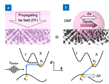
Figure 1.
Comparison of far- and near-field excitations.
-
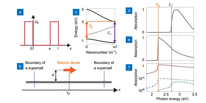
Figure 2.
ONF excitation in indirect band-gap structure.
-
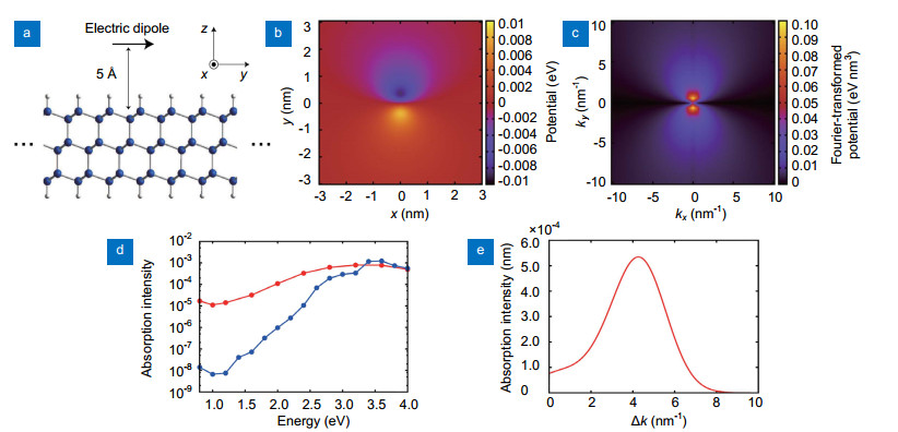
Figure 3.
ONF excitation in a realistic Si system.
-
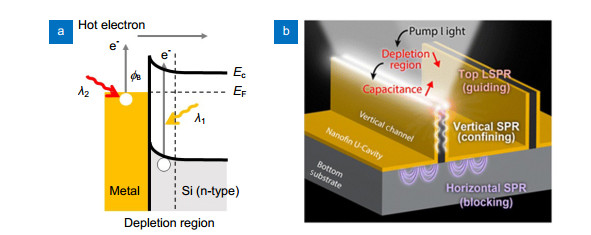
Figure 4.
Schematic of the hot electron driven photocurrent over a Schottky barrier.
-
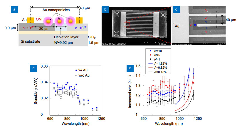
Figure 5.
Sensitivity of the lateral p–n junction with Au nanoparticles.
-
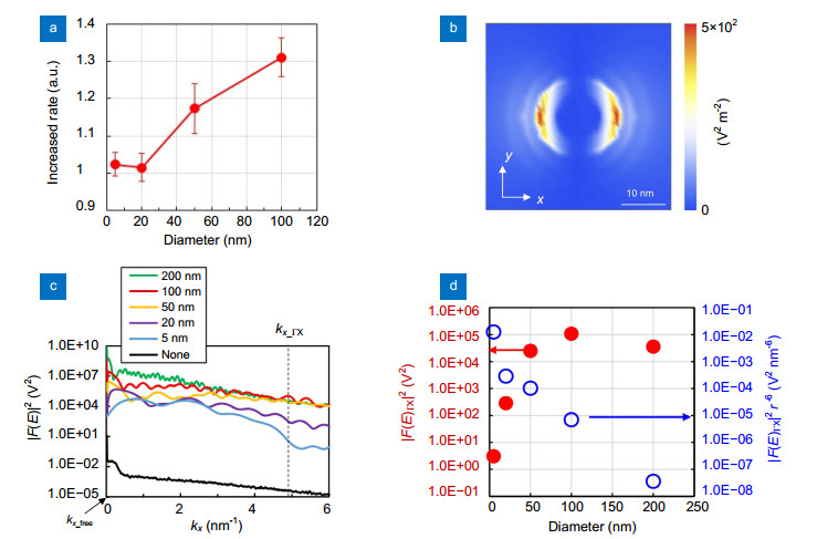
Figure 6.
Increased rate as a function of the size of Au nanoparticles.


