
 E-mail Alert
 RSS
RSS
-
摘要:
飞秒激光利用其超快的作用时间、超强的峰值功率的特性,可以与半导体材料表面发生瞬态光化学反应,从而对材料进行有效的掺杂,且可以实现超过材料固溶度极限的过饱和掺杂,同时能在材料表面形成准周期的微纳结构。导致半导体表面性质发生改变,产生超宽光谱高吸收的特性,从而突破传统物理限制,并由此产生了一系列全新的应用。本文总结了飞秒激光与硅相互作用的基本理论和几种物理模型,介绍了其在相关领域的应用,并对飞秒激光过饱和掺杂及改性硅的发展前景作出展望。
Abstract:Femtosecond laser pulses induce intriguing transient photochemical reactions with semiconductors at the sample surface, due to its ultrashort duration and ultrahigh peak power. Taking advantage of these characteristics, material can be effectively doped. The doping level is likely far beyond the solid solubility limit (so called supersaturated doping), meanwhile quasi-periodic structures with micro/nano-scales are created at the material surface as well. As a result, surface properties are strikingly changed, e.g. ultra-high absorption over a broad range from near ultraviolet to infrared emerges, which breaks the limit of traditional physics and brings novel applications. In this review, we summarize the basic theories and several physical models of femtosecond laser-silicon interaction, introduce its applications in relevant areas, and depict future prospects of femtosecond laser hyperdoped and processed silicon.
-
Key words:
- hyperdoping /
- femtosecond laser doping /
- femtosecond laser processing /
- silicon
-

Abstract: Silicon one of the most abundant elements in the earth's crust has a large impact on modern industry. It is an extremely versatile material with various applications ranging from solar energy to electronic devices. After decades of process, the crystalline silicon solar cell has been successfully commercialized all over the world due to its low cost and high efficiency. As the fundamental component of integrated circuits, silicon-based chips have shown outstanding performance in computers and cell phones. Surprisingly silicon is also a promising host material for the new generation of quantum devices owing to its excellent properties of spin. Definitely it is the core material and classical platform among various materials in the world. However, there are still some blocks which limit its applications, eg. The bandgap of crystalline silicon is only 1.12 eV (~1100 nm), which prohibited the usage in far-infrared range. The carrier mobility of silicon is not high enough, which limited performance of electronic devices.
Benefiting from the rapid development of ultrafast laser, those constraints mentioned above could be resolved by interaction between femtosecond laser and silicon. Femtosecond laser pulses induce intriguing transient photochemical reactions with semiconductors at the surface, owing to its ultrafast duration and ultra-high intensity. Taking advantage of these characteristics, material is effectively doped. The doping level is likely far beyond the solid solubility limit (so called supersaturated doping), in the meanwhile quasi-periodic structures with micro-/nano- scales are created at the surface of material as well. As a result, surface properties are strikingly changed, e.g. ultra-high absorption over a broad range from near ultraviolet to infrared emerges, which breaks the limit of traditional physics and brings novel applications. The excellent properties of this modified silicon material tap more potentials in the silicon-based semiconductor industry. In addition, compared with ion implantation, femtosecond hyperdoping can reduce lattice defects, and improve supersaturated substitution doping.
In this review, we summarized the ultrafast dynamics of the interaction between femtosecond laser and silicon and the physical mechanism of supersaturated doping. Based on the typical TTM (two-temperature model), the Drude model was introduced to correct the surface reflectivity, and a two-dimensional TTM-Drude model was proposed to explain the ultrafast energy transfer process. Subsequently, a competitive model was established that led to LIPSS (laser-induced periodic surface structures) formation on the silicon surface. Meanwhile, the microscopic process and physical mechanism of femtosecond laser supersaturated silicon doping had been improved through the researches of the plasma plume in silicon etching. Finally, we also introduced its applications in relevant areas, such as photoluminescence and photodetectors and depicted future prospects of femtosecond laser hyperdoped and modified silicon.
-

-
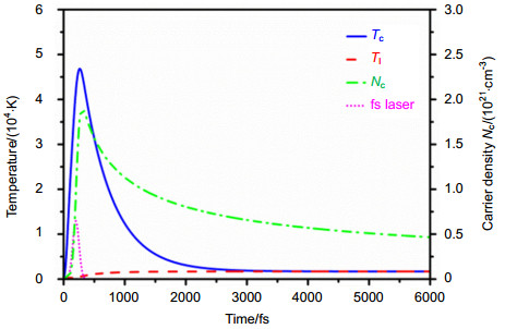
图 3 飞秒激光辐照下硅表面载流子温度(蓝色实线)、晶格温度(红色短线)以及载流子浓度(绿色点划线)随时间变化曲线,紫色点线为飞秒激光示意图[20].
Figure 3. Evolution of carrier temperature (blue solid curve), lattice temperature (red dash curve) and carrier density (green dash dot curve) under the irradiating of femtosecond. The purple dot curve shows the femtosecond laser pulse[20].
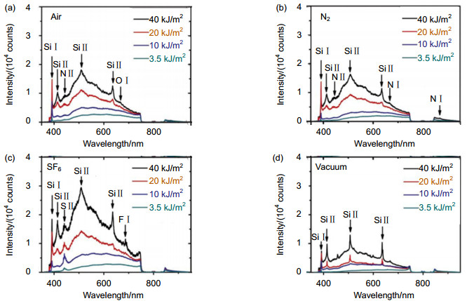
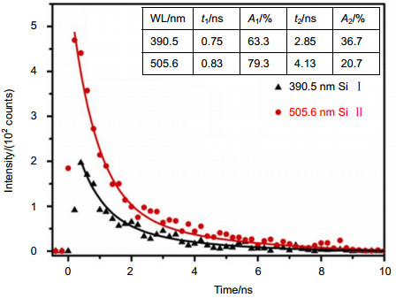
图 8 在SF6中10 kJ/m2的激光通量条件下,羽流的光谱谱线390.5 nm Si Ⅰ和505.6 nm Si Ⅱ的强度衰减曲线.图中点为实验数据,曲线为理论拟合[34].
Figure 8. The decay curves of the 390.5 nm Si Ⅰ line and of the 505.6 nm Si Ⅱ line under a laser fluence of 10 kJ/m2 in SF6. The dots represent experimental data and the solid curves represent bi-exponential fits[34].
表 1 六氟化硫中不同激光通量下,谱线505.6 nm的强度衰减曲线的双指数拟合参数及连续谱在700 nm处的光谱强度衰减的单指数拟合参数[34].
Table 1. Lifetimes of the two decay components of the 505.6 nm line and the lifetime of the continuum spectrum at 700 nm in SF6[34].
Laser fluence/(kJ/m2) τ1/ns A1/(%) τ2/ns A2/(%) τ0/ns 3.5 0.54 87.0 2.49 13.0 0.64 10 0.83 79.3 4.13 20.7 0.87 20 1.10 77.8 5.49 22.2 1.21 40 2.43 69.5 11.3 30.5 2.67  下载: 导出CSV
-
[1] Ertekin E, Winkler M T, Recht D, et al. Insulator-to-metal transition in selenium-hyperdoped silicon: observation and origin[J]. Physical Review Letters, 2012, 108(2): 026401. doi: 10.1103/PhysRevLett.108.026401
[2] Sher M J. Intermediate band properties of femtosecond-laser hyperdoped silicon[D]. Cambridge, Massachusetts: Harvard University, 2013.
https://dash.harvard.edu/handle/1/11095958 [3] Sullivan J T, Simmons C B, Krich J J, et al. Methodology for vetting heavily doped semiconductors for intermediate band photovoltaics: a case study in sulfur-hyperdoped silicon[J]. Journal of Applied Physics, 2013, 114(10): 103701. doi: 10.1063/1.4820454
[4] Ji Xu, Jiang Lan, Li Xiaowei, et al. Femtosecond laser-induced cross-periodic structures on a crystalline silicon surface under low pulse number irradiation[J]. Applied Surface Science, 2015, 326: 216–221. doi: 10.1016/j.apsusc.2014.11.124
[5] Gimpel T, Guenther K M, Kontermann S, et al. Current-voltage characteristic and sheet resistances after annealing of femtosecond laser processed sulfur emitters for silicon solar cells[J]. Applied Physics Letters, 2014, 105(5): 053504. doi: 10.1063/1.4892474
[6] Tull B R. Femtosecond laser ablation of silicon: nanoparticles, doping and photovoltaics[D]. Cambridge, Massachusetts: Harvard University, 2007.
https://www.researchgate.net/publication/252253521_Femtosecond_laser_ablation_of_silicon_Nanoparticles_doping_and_photovoltaics [7] Wu C, Crouch C H, Zhao L, et al. Near-unity below-band-gap absorption by microstructured silicon[J]. Applied Physics Let-ters, 2001, 78(13): 1850–1852. doi: 10.1063/1.1358846
[8] Her T H, Finlay R J, Wu C, et al. Microstructuring of silicon with femtosecond laser pulses[J]. Applied Physics Letters, 1998, 73(12): 1673–1675. doi: 10.1063/1.122241
[9] Younkin R, Carey J E, Mazur E, et al. Infrared absorption by conical silicon microstructures made in a variety of background gases using femtosecond-laser pulses[J]. Journal of Applied Physics, 2003, 93(5): 2626–2629. doi: 10.1063/1.1545159
[10] Tull B R, Winkler M T, Mazur E. The role of diffusion in broadband infrared absorption in chalcogen-doped silicon[J]. Applied Physics A, 2009, 96(2): 327–334. doi: 10.1007/s00339-009-5200-8
[11] Crouch C H, Carey J E, Shen M, et al. Infrared absorption by sulfur-doped silicon formed by femtosecond laser irradiation[J]. Applied Physics A, 2004, 79(7): 1635–1641. https://link.springer.com/article/10.1007/s00339-004-2676-0
[12] Sheehy M A, Tull B R, Friend C M, et al. Chalcogen doping of silicon via intense femtosecond-laser irradiation[J]. Materials Science and Engineering: B, 2007, 137(1–3): 289–294. doi: 10.1016/j.mseb.2006.10.002
[13] Shao Hezhu, Li Yuan, Zhang Jinhu, et al. Physical mechanisms for the unique optical properties of chalcogen-hyperdoped silicon[J]. Europhysics Letters, 2012, 99(4): 46005. doi: 10.1209/0295-5075/99/46005
[14] Mo Yina, Bazant M Z, Kaxiras E. Sulfur point defects in crystalline and amorphous silicon[J]. Physical Review B, 2004, 70(20): 205210. doi: 10.1103/PhysRevB.70.205210
[15] Sanchez K, Aguilera I, Palacios P, et al. Formation of a reliable intermediate band in Si heavily coimplanted with chalcogens (S, Se, Te) and group Ⅲ elements (B, Al)[J]. Physical Review B, 2010, 82(16): 165201. doi: 10.1103/PhysRevB.82.165201
[16] Sundaram S K, Mazur E. Inducing and probing non-thermal transitions in semiconductors using femtosecond laser puls-es[J]. Nature Materials, 2002, 1(4): 217–224. doi: 10.1038/nmat767
[17] Anisimov S I, Kapeliovich B L, Perel'man T L. Electron emis-sion from metal surfaces exposed to ultrashort laser pulses[J]. Zhurnal Eksperimentalnoi i Teoreticheskoi Fiziki, 1974, 39(2): 375–377.
[18] Lee S H, Lee J S, Park S, et al. Numerical analysis on heat transfer characteristics of a silicon film irradiated by pico-to femtosecond pulse lasers[J]. Numerical Heat Transfer, Part A: Applications, 2003, 44(8): 833–850. doi: 10.1080/716100525
[19] Sim H S, Lee S H, Kang K G. Femtosecond pulse laser interactions with thin silicon films and crater formation considering optical phonons and wave interference[J]. Microsystem Technologies, 2008, 14(9–11): 1439–1446. doi: 10.1007/s00542-007-0554-3
[20] 杨明. 飞秒激光诱导硅表面微纳结构研究[D]. 天津: 南开大学, 2014: 25–62.
Yang Ming. Femtosecond laser induced micro-/nano-structures on silicon[D]. Tianjin: Nankai University, 2014: 25–62.
http://cdmd.cnki.com.cn/article/cdmd-10055-1015528876.htm [21] Cavalleri A, Sokolowski-Tinten K, Bialkowski J, et al. Femto-second melting and ablation of semiconductors studied with time of flight mass spectroscopy[J]. Journal of Applied Physics, 1999, 85(6): 3301–3309. doi: 10.1063/1.369675
[22] Yang Ming, Wu Qiang, Chen Zhandong, et al. Generation and erasure of femtosecond laser-induced periodic surface structures on nanoparticle-covered silicon by a single laser pulse[J]. Optics Letters, 2014, 39(2): 343–346. doi: 10.1364/OL.39.000343
[23] Huang Min, Zhao Fuli, Cheng Ya, et al. Origin of laser-induced near-subwavelength ripples: interference between surface plasmons and incident laser[J]. ACS Nano, 2009, 3(12): 4062–4070. doi: 10.1021/nn900654v
[24] Bonse J, Rosenfeld A, Krüger J. On the role of surface plasmon polaritons in the formation of laser-induced periodic surface structures upon irradiation of silicon by femtosecond-laser pulses[J]. Journal of Applied Physics, 2009, 106(10): 104910. doi: 10.1063/1.3261734
[25] Bonse J, Rosenfeld A, Kruger J. Implications of transient changes of optical and surface properties of solids during femtosecond laser pulse irradiation to the formation of la-ser-induced periodic surface structures[J]. Applied Surface Science, 2011, 257(12): 5420–5423. doi: 10.1016/j.apsusc.2010.11.059
[26] Han Yanhua, Qu Shiliang. The ripples and nanoparticles on silicon irradiated by femtosecond laser[J]. Chemical Physics Letters, 2010, 495(4–6): 241–244. doi: 10.1016/j.cplett.2010.06.071
[27] Garrelie F, Colombier J P, Pigeon F, et al. Evidence of surface plasmon resonance in ultrafast laser-induced ripples[J]. Optics Express, 2011, 19(10): 9035–9043. doi: 10.1364/OE.19.009035
[28] Maier S A. Plasmonics: fundamentals and applications[M]. Boston, MA: Springer Science & Business Media, 2007.
[29] Silvestrelli P L, Alavi A, Parrinello M, et al. Ab initio molecular dynamics simulation of laser melting of silicon[J]. Physical Review Letters, 1996, 77(15): 3149–3152. doi: 10.1103/PhysRevLett.77.3149
[30] Roeterdink W G, Juurlink L B F, Vaughan O P H, et al. Coulomb explosion in femtosecond laser ablation of Si(111)[J]. Applied Physics Letters, 2003, 82(23): 4190–4192. doi: 10.1063/1.1580647
[31] Stoian R, Rosenfeld A, Hertel I V, et al. Comment on "Coulomb explosion in femtosecond laser ablation of Si(111)"[Appl. Phys. Lett. 82, 4190 (2003)][J]. Applied Physics Letters, 2004, 85(4): 694–695. doi: 10.1063/1.1771817
[32] Amoruso S, Bruzzese R, Spinelli N, et al. Generation of silicon nanoparticles via femtosecond laser ablation in vacuum[J]. Applied Physics Letters, 2004, 84(22): 4502–4504. doi: 10.1063/1.1757014
[33] Wu Zehua, Zhang Nan, Wang Mingwei, et al. Femtosecond laser ablation of silicon in air and vacuum[J]. Chinese Optics Letters, 2011, 9(9): 093201. doi: 10.3788/COL
[34] Chen Zhandong, Wu Qiang, Yang Ming, et al. Generation and evolution of plasma during femtosecond laser ablation of silicon in different ambient gases[J]. Laser and Particle Beams, 2013, 31(3): 539–545. doi: 10.1017/S0263034613000281
[35] 陈战东. 飞秒激光改性硅材料的物理机理及其性质研究[D]. 天津: 南开大学, 2014: 58–79.
Chen Zhandong. Study on the mechanisms and the properties of femtosecond-laser processing silicon[D]. Tianjin: Nankai University, 2014: 58–79.
http://cdmd.cnki.com.cn/Article/CDMD-10055-1015528854.htm [36] Stuart B C, Feit M D, Herman S, et al. Nanosecond-to-femtosecond laser-induced breakdown in dielectrics[J]. Physical Review B, 1996, 53(4): 1749–1761. doi: 10.1103/PhysRevB.53.1749
[37] Wendelen W, Mueller B Y, Autrique D, et al. Space charge corrected electron emission from an aluminum surface under non-equilibrium conditions[J]. Journal of Applied Physics, 2012, 111(11): 113110. doi: 10.1063/1.4729071
[38] Chuang T J. Multiple photon excited SF6 interaction with silicon surfaces[J]. The Journal of Chemical Physics, 1981, 74(2): 1453–1460. doi: 10.1063/1.441132
[39] 刘恩科, 朱秉升, 罗晋生.半导体物理学[M].北京:国防工业出版社, 1979.
Liu Enke, Zhu Bingsheng, Luo Jinsheng. The physics of semiconductors[M]. Beijing: National Defense Industry Press, 1979.
[40] Zheng B, Michel J, Ren F Y G, et al. Room‐temperature sharp line electroluminescence at λ=1.54 μm from an erbium‐doped, silicon light‐emitting diode[J]. Applied Physics Letters, 1994, 64(21): 2842–2844. doi: 10.1063/1.111977
[41] Svrcek V, Sasaki T, Shimizu Y, et al. Blue luminescent silicon nanocrystals prepared by ns pulsed laser ablation in water[J]. Applied Physics Letters, 2006, 89(21): 213113. doi: 10.1063/1.2397014
[42] Wu C, Crouch C H, Zhao L, et al. Visible luminescence from silicon surfaces microstructured in air[J]. Applied Physics Let-ters, 2002, 81(11): 1999–2001. doi: 10.1063/1.1504868
[43] 朱世伟, 王磊, 陈兴, 等.脉冲激光烧蚀法制备硅纳米颗粒及其光致发光特征[J].中国激光, 2010, 37(3): 882–886. http://www.cqvip.com/QK/95389X/201003/33366363.html
Zhu Shiwei, Wang Lei, Chen Xing, et al. Synthesis and photoluminescence of silicon nanoparticles fabricated by pulse laser ablation[J]. Chinese Journal of Lasers, 2010, 37(3): 882–886. http://www.cqvip.com/QK/95389X/201003/33366363.html
[44] Emelyanov A V, Kazanskii A G, Khenkin M V, et al. Visible luminescence from hydrogenated amorphous silicon modified by femtosecond laser radiation[J]. Applied Physics Letters, 2012, 101(8): 081902. doi: 10.1063/1.4747207
[45] Lü Quan, Wang Jian, Liang Cong, et al. Strong infrared photoluminescence from black silicon made with femtosecond laser irradiation[J]. Optics Letters, 2013, 38(8): 1274–1276. doi: 10.1364/OL.38.001274
[46] Chen Zhandong, Wu Qiang, Yang Ming, et al. Time-resolved photoluminescence of silicon microstructures fabricated by femtosecond laser in air[J]. Optics Express, 2013, 21(18): 21329–21336. doi: 10.1364/OE.21.021329
[47] Huang Zhihong, Carey J E, Liu Mingguo, et al. Microstructured silicon photodetector[J]. Applied Physics Letters, 2006, 89(3): 033506. doi: 10.1063/1.2227629
[48] Li X, Carey J E, Sickler J W, et al. Silicon photodiodes with high photoconductive gain at room temperature[J]. Optics Express, 2012, 20(5): 5518–5523. doi: 10.1364/OE.20.005518
[49] 冯国进. 飞秒激光微构造硅光学性质研究及实验装置[D]. 上海: 复旦大学, 2010.
Feng Guojin. Optical properties of micro-structured silicon by femtosecond laser and equipment[D]. Shanghai: Fudan University, 2010.
http://cdmd.cnki.com.cn/article/cdmd-10246-1012330807.htm [50] 李媛. 飞秒激光微构造硅的光电性质研究[D]. 上海: 复旦大学, 2012.
Li Yuan. Optical properties of micro-structured silicon by femtosecond laser[D]. Shanghai: Fudan University, 2012.
http://cdmd.cnki.com.cn/Article/CDMD-10246-1013100615.htm [51] 吕振华. 红外吸收增强黑硅材料的研究与制备[D]. 长春: 吉林大学, 2013.
Lü Zhenhua. Fabrication and investigation of black silicon of enhanced near-infrared absorption[D]. Changchun: Jilin Uni-versity, 2013.
http://cdmd.cnki.com.cn/Article/CDMD-10183-1013193026.htm [52] Zhao Li, Wu Qiang, Zeng Qiang, et al. Sulfur-hyperdoped silicon photodetector with broadband spectral response and high gain at low bias[C]//Proceedings of 2016 Conference on Lasers and Electro-Optics, 2016: 1–2.
https://ieeexplore.ieee.org/abstract/document/7788047/ -
 点击扫一扫
点击扫一扫
图(12)
表(1)
计量
- 文章访问数: 9043
- PDF下载数: 4677
- 施引文献: 0


