
 E-mail Alert
 RSS
RSS
| Citation: |
Wang Weimin, Wang Qiang. Development and characterization of a 140-element MEMS deformable mirror[J]. Opto-Electronic Engineering, 2018, 45(3): 170698. doi: 10.12086/oee.2018.170698

|
Development and characterization of a 140-element MEMS deformable mirror
-
Abstract
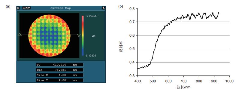
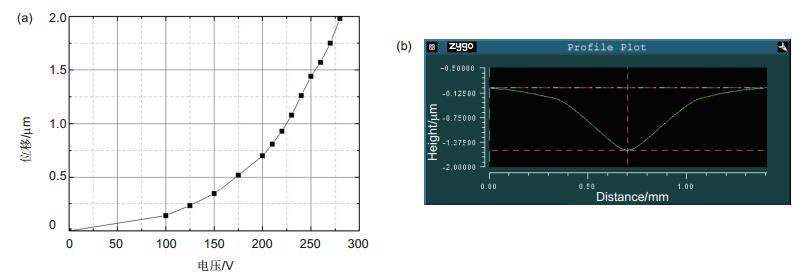
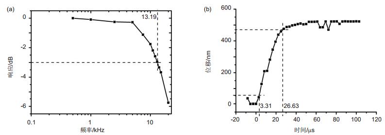
For satisfying the boarder application requirement of adaptive optics (AO) and solving the problem of large volume and high cost of conventional deformable mirrors (DM), micro DM based on micro-electro-mechanical system (MEMS) technology is developed and measured. The developed DM has 140 hexagonal parallel plate capacitor electrostatic actuators. The actuators are arranged as a square array and the pitch is 400 μm. A DM prototype is fabricated by MEMS surface micromachining process and packaged by a ceramic pin grid array (CPGA). A miniaturization multi-channel high voltage driver for the DM is developed too. The measurement results show that the prototype has a surface PV value of 411 nm, RMS value of 78 nm, reflectivity of about 80% in 600 nm to 900 nm wavelength, stroke of 1.8 μm, actuator coupling of 15%, working bandwidth of 13 kHz and step response time of 23 μs. Thus the DM has the advantages of small volume, low cost and fast response. Besides the measurement of single element, the whole DM is controlled open loop to fit Zernike aberration and its fitting capability is demonstrated. Above results indicate that the DM prototype can satisfy initially the requirement of AO system.-
Keywords:
- MEMS /
- deformable mirror /
- adaptive optics /
- electrostatic actuator
-

-
References
[1] 姜文汉, 张雨东, 饶长辉, 等.中国科学院光电技术研究所的自适应光学研究进展[J].光学学报, 2011, 31(9): 0900106. Jiang W H, Zhang Y D, Rao C H, et al. Progress on adaptive optics of institute of optics and electronics, Chinese academy of sciences[J]. Acta Optica Sinica, 2011, 31(9): 0900106. [2] Morzinski K M, Norton A P, Evans J W, et al. MEMS practice: from the lab to the telescope[J]. Proceedings of SPIE, 2012, 8253: 825304. doi: 10.1117/12.910964 [3] Manzanera S, Helmbrecht M A, Kempf C J, et al. MEMS segmented-based adaptive optics scanning laser ophthalmoscope[J]. Biomedical Optics Express, 2011, 2(5): 1204-1217. doi: 10.1364/BOE.2.001204 [4] Cornelissen S A, Bierden P A, Bifano T G, et al. 4096-element continuous face-sheet MEMS deformable mirror for high-contrast imaging[J]. Journal of Micro/Nanolithography, MEMS, and MOEMS, 2009, 8(3): 031308. doi: 10.1117/1.3158067 [5] Helmbrecht M A, He M, Kempf C J. Development of high-order segmented MEMS deformable mirrors[J]. Proceedings of SPIE, 2012, 8253: 825307. doi: 10.1117/12.912547 [6] Vdovin G, Soloviev O, Samokhin A, et al. Correction of low order aberrations using continuous deformable mirrors[J]. Optics Express, 2008, 16(5): 2859-2866. doi: 10.1364/OE.16.002859 [7] Dagel D J, Cowan W D, Spahn O B, et al. Large-stroke MEMS deformable mirrors for adaptive optics[J]. Journal of Microelectromechanical Systems, 2006, 15(3): 572-583. doi: 10.1109/JMEMS.2006.876794 [8] Fernández B R, Bouchti M A, Kubby J. High-stroke, high-order MEMS deformable mirrors[J]. Journal of Micro/Nanolithography, MEMS, and MOEMS, 2013, 12(3): 033012. doi: 10.1117/1.JMM.12.3.033012 [9] Jung I W, Peter Y A, Carr E, et al. Single-crystal-silicon continuous membrane deformable mirror array for adaptive optics in space-based telescopes[J]. IEEE Journal of Selected Topics in Quantum Electronics, 2007, 13(2): 162-167. [10] Yu H B, Chen H Q. Development of a novel micromirror based on surface micromaching technology[J]. Sensors and Actuators A: Physical, 2006, 125(2): 458-462. doi: 10.1016/j.sna.2005.06.020 [11] Qiao D Y, Wang S J, Yuan W Z. A continuous-membrane micro deformable mirror based on anodic bonding of SOI to glass wafer[J]. Microsystem Technologies, 2010, 16(10): 1765-1769. doi: 10.1007/s00542-010-1102-0 [12] 乔大勇, 刘耀波, 王松洁, 等.基于微机电系统技术的分立式微变形镜[J].航空精密制造技术, 2010, 46(4): 6-12. Qiao D Y, Liu Y B, Wang S J, et al. Segmented micro deformable mirrors based on MEMS technology[J]. Aviation Precision Manufacturing Technology, 2010, 46(4): 6-12. [13] Sun Q, He K, Cretu E. Optimization designed large-stroke MEMS micromirror for adaptive optics[J]. Chinese Optics Letters, 2010, 8(12): 1163-1166. doi: 10.3788/COL [14] Chen D S, Yeh P F, Chen Y F, et al. An electrothermal actuator with two degrees of freedom serving as the arm of a MEMS gripper[J]. IEEE Transactions on Industrial Electronics, 2014, 61(10): 5465-5471. doi: 10.1109/TIE.2013.2293693 [15] Ma J Q, Liu Y, Chen C P, et al. Deformable mirrors based on piezoelectric unimorph microactuator array for adaptive optics correction[J]. Optics Communications, 2011, 284(21): 5062-5066. doi: 10.1016/j.optcom.2011.07.021 [16] Zhang W M, Yan H, Peng Z K, et al. Electrostatic pull-in instability in MEMS/NEMS: A review[J]. Sensors and Actuators A: Physical, 2014, 214: 187-218. doi: 10.1016/j.sna.2014.04.025 [17] Wang W M, Tao F G, Zhang J F, et al. A 19 element hexagonal actuator arrangement continuous face-sheet MEMS deformable mirror[J]. Key Engineering Materials, 2012, 503: 169-173. doi: 10.4028/www.scientific.net/KEM.503 [18] 汪为民. 表面工艺静电驱动MEMS变形镜关键技术研究[D]. 成都: 电子科技大学, 2015: 33-37. Wang W M. Research on key technologies of surface-micromachined electrostatic actuated MEMS deformable mirrors[D]. Chengdu: University of Electronic Science and Technology of China, 2015: 33-37. http://www.wanfangdata.com.cn/details/detail.do?_type=degree&id=D665534 [19] Hudgin R. Wave-front compensation error due to finite corrector-element size[J]. Journal of the Optical Society of America, 1977, 67(3): 393-395. doi: 10.1364/JOSA.67.000393 [20] 钱劲, 刘澂, 张大成, 等.微电子机械系统中的残余应力问题[J].机械强度, 2001, 23(4): 393-401. Qian J, Liu C, Zhang D C, et al. Residual stresses in micro-electro-mechanical systems[J]. Journal of Mechanical Strength, 2001, 23(4): 393-401. [21] 代永平, 耿卫东, 孙钟林, 等. CMP平坦化技术在LCoS显示器中的应用[J].光电子技术, 2003, 23(1): 41-45. Dai Y P, Geng W D, Sun Z L, et al. Application of CMP planarization in LCoS[J]. Optoelectronic Technology, 2003, 23(1): 41-45. [22] Mali R K, Bifano T, Koester D. A design-based approach to planarization in multilayer surface micromachining[J]. Journal of Micromechanics and Microengineering, 1999, 9(4): 294-299. doi: 10.1088/0960-1317/9/4/302 [23] 凌宁, 官春林.变形反射镜的发展[J].光电工程, 1995, 22(1): 14-22. Ling N, Guan C L. The development of deformable mirrors[J]. Opto-Electronic Engineering, 1995, 22(1): 14-22. -
Overview

Overview: Adaptive optics (AO) technology is an important method to compensate optical wavefront aberration caused by atmosphere turbulence and deformable mirror (DM), whose surface can be tuned dynamically, is one of its key components. For satisfying the boarder application requirement of AO technology and solving the problem of large volume and high cost of conventional piezoelectric DMs, micro DM based on micro-electro-mechanical system (MEMS) technology is developed and measured. Due to its low power consumption, zero hysteresis, and good integrated circuit (IC) compatibility, parallel plate capacitor electrostatic actuator is adopted to actuate the MEMS DM. The developed DM has 140 hexagonal parallel plate actuators, which has a larger stroke and higher frequency when compared to square parallel plate actuators. The stroke, pull-in voltage, one order natural frequency, and Euler critical stress of the actuator are simulated and compared by finite element analysis (FEA). The actuators are arranged as a 12×12 square array and the pitch is 400 μm. The facesheet of the DM is a continuous square membrane with an area of 4.4 mm×4.4 mm. A DM prototype is fabricated by MEMS surface micromachining process. The material for structural layer and sacrificial layer of the process are polysilicon and phosphosilicate glass (PSG), respectively. The whole process includes three structural layers and two sacrificial layers. The three structural layers are the lower electrode, the upper electrode and the facesheet, respectively. The fabricated DM prototype is packaged by a ceramic pin grid array (CPGA) and a quartz glass lid. A miniaturization multichannel high voltage driver for the DM is developed at the same time. The optical and electromechanical, including static and dynamic, performances of the prototype are measured by a Zygo NewView 7300 noncontact white light profiler. The measurement results show that the prototype has a surface PV value of 411 nm, RMS value of 78 nm, reflectivity of about 80% in 600 nm to 900 nm wavelength, stroke of 1.8 μm, actuator coupling of 15%, working bandwidth of 13 kHz and step response time of 23 μs. Thus the DM has the advantages of small volume, low cost and fast response. Besides the measurement of single element, the whole DM is controlled open loop to fit Zernike aberration and its fitting capability is demonstrated. Above results indicate that the DM prototype can satisfy preliminarily the requirement of AO system and promote its applications in civil market, such as ophthalmoscope and free space optical communication.
-
Access History
Figures(9)
Tables(1)
Article Metrics

Export File
Citation
Wang Weimin, Wang Qiang. Development and characterization of a 140-element MEMS deformable mirror[J]. Opto-Electronic Engineering, 2018, 45(3): 170698. doi: 10.12086/oee.2018.170698
Format
Content
 DownLoad:
-
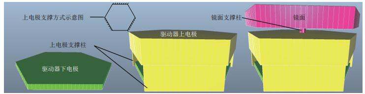
Figure 1.
Hexagonal electrostatic parallel plate actuator and facesheet
-
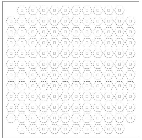
Figure 2.
Actuator geometry of the 140-element MEMS DM
-
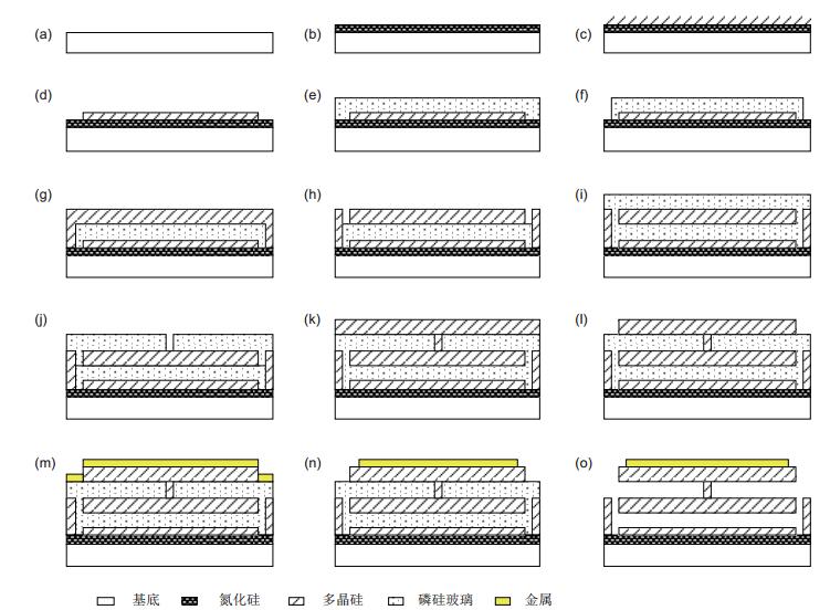
Figure 3.
MEMS surface micromachining process
-
Figure 4.
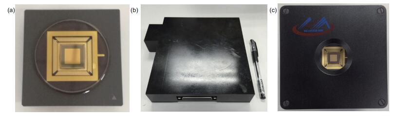
(a) The MEMS DM after package; (b) 192-channel high speed driver; (c) The photograph of the DM prototype
-
Figure 5.
(a) Measured surface profile; (b) Test curve of reflectivity
-
Figure 6.
(a) Measured stroke; (b) The cross section of deformed surface
-
Figure 7.
(a) Measured bandwidth; (b) Step response time
-
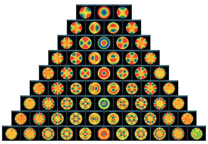
Figure 8.
Open loop fitting of the 3rd to 65th term Zernike aberation
-
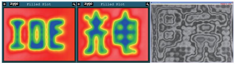
Figure 9.
The surface profile and interference fringe of some patterns fitted by the DM


