
 E-mail Alert
 RSS
RSS
| Citation: |
Wang Hao, Dong Lianhe, Zhu Guodong, et al. Fabrication method of quartz aspheric microlens array for turning mask[J]. Opto-Electronic Engineering, 2018, 45(4): 170671. doi: 10.12086/oee.2018.170671

|
Fabrication method of quartz aspheric microlens array for turning mask
-
Abstract
In order to solve the two difficult problems of the poor processing controllability and the low surface accuracy of quartz aspheric microlens array processing, a fabrication method of quartz aspheric microlens array for turning mask is proposed. This method mainly uses single point diamond turning technology and reactive ion etching technology, studies the turning and etching properties of the mask material, and optimizes the mask material by experiment. Finally, the fabrication of an aspherical glass microlens array with an area of 5 mm×5 mm was carried out. The experimental results are compared with the expected parameters. The analysis shows that the error root mean square of the quartz glass component is 1.155 nm, and the surface accuracy error is 0.47%.-
Keywords:
- mask /
- quartz glass /
- aspheric microlens array /
- SPDT /
- RIE
-

-
References
[1] 杨桂栓, 陈涛, 陈虹. 248 nm准分子激光刻蚀的无裂损石英玻璃表面微通道[J].中国激光, 2017, 44(9): 0902004. Yang G S, Chen T, Chen H. Crack-free silica glass surface micro-grooves etched by 248 nm excimer lasers[J]. Chinese Journal of Lasers, 2017, 44(9): 0902004. [2] Zhang J, Sugioka K, Takahashi T, et al. Dual-beam ablation of fused silica by multiwavelength excitation process using KrF excimer and F2 lasers[J]. Applied Physics A, 2000, 71(1): 23-26. [3] 崔铮.微纳米加工技术及其应用[M]. 3版.北京:高等教育出版社, 2013: 24-32. Cui Z. Micro-nanofabrication Technologies and Applications[M]. 3rd ed. Beijing: Higher Education Press, 2013: 24-32. [4] 张健, 代雷, 王飞, 等.小磨头自适应抛光抑制高精度非球面中频误差[J].光学学报, 2013, 33(8): 0822002. Zhang J, Dai L, Wang F, et al. Restraint of mid-spatial-frequency error aspheric surface by small-tool adaptive polishing[J]. Acta Optica Sinica, 2013, 33(8): 0822002. [5] Ridge M T, Cox D C, Webb R P, et al. The fabrication of aspherical microlenses using focused ion-beam techniques[J]. Micron, 2014, 57: 56-66. doi: 10.1016/j.micron.2013.10.013 [6] Yuan W, Chan C Y, Li L H, et al. Investigation of the surface profile along the cutting trajectory and its correlation with cutting forces in single point diamond turning[J]. The International Journal of Advanced Manufacturing Technology, 2017, 89(5-8): 1327-1338. doi: 10.1007/s00170-016-9087-1 [7] 王毅, 余景池.超精密车削金刚石刀具刃口误差的高精度补偿[J].光电工程, 2011, 38(1): 98-102. Wang Y, Yu J C. Compensation for error of diamond tool's cutting edge in single diamond turning[J]. Opto-Electronic Engineering, 2011, 38(1): 98-102. [8] Gong L B, Cheung C F. Modeling and characterization of surface generation in fast tool servo machining of microlens arrays[J]. Computers & Industrial Engineering, 2012, 63(4): 957-970. [9] Dunkel J, Wippermann F, Brückner A, et al. Fabrication of refractive freeform array masters for artificial compound eye cameras[J]. Proceedings of SPIE, 2014, 9130: 91300P. doi: 10.1117/12.2054596 [10] Mukaida M, Yan J W. Ductile machining of single-crystal silicon for microlens arrays by ultraprecision diamond turning using a slow tool servo[J]. International Journal of Machine Tools and Manufacture, 2017, 115: 2-14. doi: 10.1016/j.ijmachtools.2016.11.004 [11] Chen Y L, Cai Y D, Tohyama K, et al. Auto-tracking single point diamond cutting on non-planar brittle material substrates by a high-rigidity force controlled fast tool servo[J]. Precision Engineering, 2017, 49: 253-261. doi: 10.1016/j.precisioneng.2017.02.014 [12] 闫锋, 范镝, 张斌智, 等.一种SiC非回转对称非球面的加工与检测[J].光电工程, 2009, 36(3): 135-139. Yan F, Fan D, Zhang B Z, et al. Manufacturing and testing of a SiC unrotational-symmetric aspherical optics[J]. Opto-Electronic Engineering, 2009, 36(3): 135-139. [13] 朱海丰, 贾翠萍, 方志良.非球面人工晶体设计及其光学性能研究[J].光电工程, 2009, 36(4): 56-59. Zhu H F, Jia C P, Fang Z L. Design method and optical performance of aspherical IOL[J]. Opto-Electronic Engineering, 2009, 36(4): 56-59. [14] 恩德, 徐可欣, 陈才和, 等.集成光学非球面消球差双凸波导透镜的研制[J].光电工程, 2008, 35(10): 98-101, 115. En D, Xu K X, Chen C H, et al. Development of integrated optical aplanatic double-convex aspherical waveguide lens[J]. Opto-Electronic Engineering, 2008, 35(10): 98-101, 115. [15] 张少峰, 刘正堂, 李阳平, 等.反应离子刻蚀法制备石英纳米压印模板的工艺研究[J].机械科学与技术, 2012, 31(11): 1786-1789. Zhang S F, Liu Z T, Li Y P, et al. Preparation and characterization of nanoimprint template on quartz by reactive ion etching[J]. Mechanical Science and Technology for Aerospace Engineering, 2012, 31(11): 1786-1789. [16] Chiromawa N L, Ibrahim K. Fabrication of micro-array of Fresnel rings on Si by electron beam lithography and reactive ion etching[J]. Applied Physics A, 2016, 122(2): 129. doi: 10.1007/s00339-016-9649-y [17] 谢玉萍, 吴鹏, 杨正, 等.基于移动掩模曝光的聚酰亚胺连续微结构刻蚀工艺研究[J].光子学报, 2015, 44(9): 0922004. Xie Y P, Wu P, Yang Z, et al. Continuous microstructure etching process polyimide based moving mask exposure[J]. Acta Photonica Sinica, 2015, 44(9): 0922004. [18] Yu E, Kim S C, Lee H J, et al. Extreme wettability of nanostructured glass fabricated by non-lithographic, anisotropic etching[J]. Scientific Reports, 2015, 5: 9362. doi: 10.1038/srep09362 [19] Mahoney S A, Rufford T E, Rudolph V, et al. Creation of microchannels in Bowen Basin coals using UV laser and reactive ion etching[J]. International Journal of Coal Geology, 2015, 144-145: 48-57. doi: 10.1016/j.coal.2015.04.001 [20] 陆志远, 胡国华, 恽斌峰, 等.聚合物光波导的反应离子刻蚀工艺研究[J].微细加工技术, 2008(3): 5-9. Lu Z Y, Hu G H, Yun B F, et al. RIE technological study of polymer optical waveguide[J]. Microfabrication Technology, 2008(3): 5-9. [21] 张丛春, 杨春生, 丁桂甫, 等. PMMA的反应离子深刻蚀[J].真空科学与技术学报, 2004, 24(2): 157-160. Zhang C C, Yang C S, Ding G F, et al. Deep reactive ion etching of polymethylmethacrylate[J]. Vacuum Science and Technology, 2004, 24(2): 157-160. [22] Shi L F, Du C L, Dong X C, et al. Effective formation method for an aspherical microlens array based on an aperiodic moving mask during exposure[J]. Applied Optics, 2007, 46(34): 8346-8350. doi: 10.1364/AO.46.008346 -
Overview

Overview: In the existing mature processing methods, the processing of micro optical structure can be divided into two major categories: microstructural lithography and single point diamond turning. Microstructural lithography can be used to process inorganic materials, such as quartz, silicon and so on. However, microstructural lithography has not been able to solve the problem of micro and nano structure shape control. The single point diamond turning technology can achieve precise control of the surface shape, but it is difficult to process the inorganic and brittle materials.
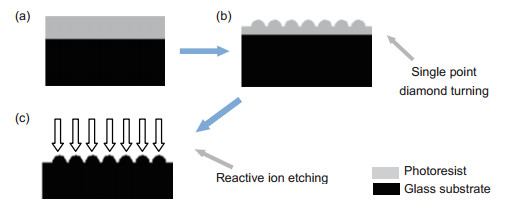
In order to solve the two difficult problems of quartz aspheric microlens array processing, such as poor controllability and low surface accuracy, a method of making quartz glass based on turning mask and etching is proposed. The single point diamond turning technology and micro photomask technology is innovatively combined. The mask layer pattern is made by single point diamond turning, and then the mask pattern is transferred by reactive ion etching. Finally the fabrication of quartz glass aspheric microlens array element is completed.
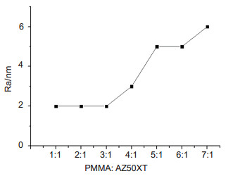
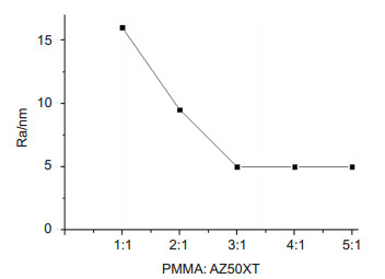
We mainly make the selection of the mask material and study the etching performance and turning performance of PMMA and AZ50XT photoresist. We find that the addition of AZ50XT photoresist in PMMA can effectively improve the anti etching performance, not only meet the requirements of single point diamond turning, and after reactive ion etching after the mask pattern can be maintained by the original still. By analyzing the surface roughness of mask after single point diamond turning and the surface roughness of mask after reactive ion etching, we get the most suitable mask material for this processing method. Finally, the new material is used to make the mask. The pattern is made on the mask surface by single point diamond turning, and the mask pattern is transferred to the quartz substrate by reactive ion etching technology. The aspheric microlens array with area of 5 mm×5 mm is obtained.
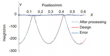
The experimental results are compared with the expected parameters. The analysis shows that the root mean square error of the quartz glass element manufactured by this method is 1.155 nm and the accuracy of face shape error is 0.47%. The experimental results show that this method possesses not only the advantages of single point diamond turning technology, such as high surface accuracy, high processing stability and mature technology, but good anisotropy of reactive ion etching technology. This method has great potential for development, and it also provides a strong support for the wider application of quartz glass materials.
-
Access History

Export File
Citation
Wang Hao, Dong Lianhe, Zhu Guodong, et al. Fabrication method of quartz aspheric microlens array for turning mask[J]. Opto-Electronic Engineering, 2018, 45(4): 170671. doi: 10.12086/oee.2018.170671
Format
Content
 DownLoad:
-
Figure 1.
Fabrication method of aspheric microlens array based on turning mask
-
Figure 2.
Surface roughness curves of masking materials with different parameters after etching
-
Figure 3.
Surface roughness curves of masking materials with different parameters after turning
-
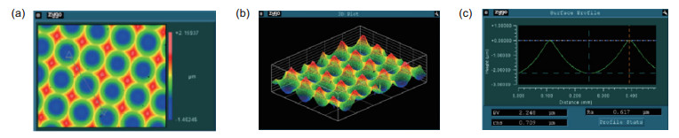
Figure 4.
Test results of aspheric microlens array
-
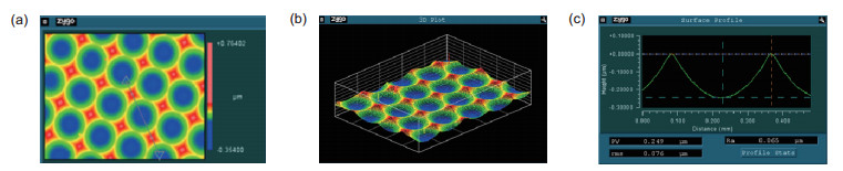
Figure 5.
Test results of quartz glass elements
-
Figure 6.
Comparison of the expected cross section of micromirror and the cross section of the micromirror after processing


