
 E-mail Alert
 RSS
RSS
| Citation: |
Kong Mingdong, Li Bincheng, Guo Chun, et al. Characterictics of absorption edge of SiO2 films[J]. Opto-Electronic Engineering, 2019, 46(4): 180220. doi: 10.12086/oee.2019.180220

|
Characterictics of absorption edge of SiO2 films
-
Abstract
Silicon dioxide (SiO2) is one of the most widely used in various optical system as film material. The micro-structure and defects of SiO2 films are of great importance to the functions and performance of these optical systems. In this paper, the absorption edge characteristics of single layer SiO2 films prepared by electron beam evaporation, ion assisted deposition, and magnetron sputtering are investigated in detail via calculating their absorption edge spectrum, which is divided into three regions: the strong absorption, exponential absorption, and weak absorption regions. The bandgap, Urbach tail, and concentration of oxygen deficiency centers (ODC) are obtained by analyzing the measured absorption spectrum. By analyzing the bandgap, Urbach tail, and ODC data of SiO2 films prepared with different deposition techniques and annealed at different temperatures, the atomic arrangement as well as micro-defect information of SiO2 films are obtained and compared. Such information of SiO2 films are important to the preparation of high-performance optical coatings employing SiO2 as the low refractive index material.-
Keywords:
- SiO2 film /
- bandgap /
- Urbach tail energy /
- oxygen deficiency centers
-

-
References
[1] Dijon J, Rafin B, Pelle C, et al. One-hundred joule per square centimeter 1.06-μm mirrors[J]. Proceedings of SPIE, 2000, 3902: 158-168. doi: 10.1117/12.379321 [2] Scherer K, Nouvelot L, Lacan P, et al. Optical and mechanical characterization of evaporated SiO2 layers. Long-term evolution[J]. Applied Optics, 1996, 35(25): 5067-5072. doi: 10.1364/AO.35.005067 [3] 季一勤.离子束溅射高性能SiO2薄膜特性研究[D].哈尔滨: 哈尔滨工业大学, 2013: 68-94. Ji Y Q, Investigation of high performance SiO2 thin film prepared by ion beam sputtering deposition[D]. Harbin Institute of Technology, 2013: 68-94. http://cdmd.cnki.com.cn/Article/CDMD-10213-1014084927.htm [4] Beauville F, Buskulic D, Flaminio R, et al. Low-loss coatings for the VIRGO large mirrors[J]. Proceedings of SPIE, 2004, 5250: 483-492. doi: 10.1117/12.516431 [5] Lorenzi R, Brovelli S, Meinardi F, et al. Role of sol-gel networking and fluorine doping in the silica Urbach energy[J]. Journal of Non-Crystalline Solids, 2011, 357(8-9): 1838-1841. doi: 10.1016/j.jnoncrysol.2010.12.051 [6] Kranjčec M, Studenyak I P, Kurik M V. On the Urbach rule in non-crystalline solids[J]. Journal of Non-Crystalline Solids, 2009, 355(1): 54-57. doi: 10.1016/j.jnoncrysol.2008.03.051 [7] Skuja L, Kajihara K, Ikuta Y, et al. Urbach absorption edge of silica: reduction of glassy disorder by fluorine doping[J]. Journal of Non-Crystalline Solids, 2004, 345-346: 328-331. doi: 10.1016/j.jnoncrysol.2004.08.038 [8] Al-Ani S K J, Arshak K I, Hogarth C A. The optical absorption edge of amorphous thin films of silicon monoxide[J]. Journal of Materials Science, 1984, 19(6): 1737-1748. doi: 10.1007/BF00550243 [9] Palik E D. Handbook of optical constants of solids[M]. Academic press, 1998: 749-759. [10] Guo C, Kong M D, Lin D W, et al. Determination of optical constants in DUV/VUV[J]. Chinese Optics Letters, 2013, 11(10): S10607. [11] 郭春, 林大伟, 张云洞, 等.光度法确定LaF3薄膜光学常数[J].光学学报, 2011, 31(7): 0731001. Guo C, Lin D W, Zhang Y D, et al. Determination of optical constants of LaF3 films from spectrophotometric measurements[J]. Acta Optica Sinica, 2011, 31(7): 0731001. [12] 黄昆.固体物理学[M].北京:高等教育出版社, 1988. Huang K. Solid State Physics[M]. Beijing: Higher Education Press, 1988. [13] Skuja L. Optically active oxygen-deficiency-related centers in amorphous silicon dioxide[J]. Journal of Non-Crystalline Solids, 1998, 239(1-3): 16-48. doi: 10.1016/S0022-3093(98)00720-0 [14] Skuja L, Hosono H, Hirano M. Laser-induced color centers in silica[J]. Proceedings of SPIE, 2001, 4347: 155-168. doi: 10.1117/12.425020 [15] Pacchioni G, Skuja L, Griscom D L. Defects in SiO2 and Related Dielectrics: Science and Technology[M]. Dordrecht: Springer, 2000: 73-116. [16] Revesz A G, Hughes H L. The structural aspects of non-crystalline SiO2 films on silicon: a review[J]. Journal of Non-Crystalline Solids, 2003, 328(1-3): 48-63. doi: 10.1016/S0022-3093(03)00467-8 -
Overview

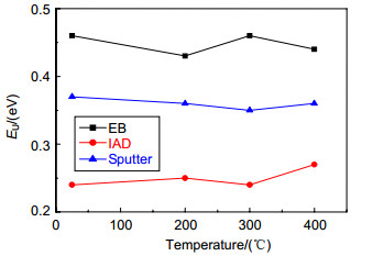
Overview: Silicon dioxide (SiO2) is one of the most widely used in various optical system as film material. The micro-structure and defects of SiO2 films are of great importance to the functions and performance of these optical systems. The absorption edge spectrum of thin film was calculated by measuring the ultraviolet spectrum curve of SiO2 thin film sample. By analyzing and calculating the strong absorption, exponential absorption, and weak absorption regions in the absorption edge spectrum of SiO2 thin film, the data of the bandgap, Urbach tail energy, and concentration of oxygen deficiency centers ODC(I) can be obtained. Based on the relationship of these experimental data to thin film micro-structure and defects, information about the atomic arrangement structure and microscopic defects of SiO2 thin film can be learned. In this paper, SiO2 films were prepared by electron beam evaporation, ion assisted deposition and magnetron sputtering. The data of the bandgap, Urbach tail energy, and ODC(I) content of raw films and films annealed at different temperatures were obtained by measurement, calculation and analysis. These data are used to understand the atomic arrangement structure and microscopic defects of SiO2 films prepared by different coating technologies and at different annealing temperatures. The structural disorder in electron beam evaporation SiO2 films is the most serious, followed by the magnetron sputtering SiO2 films, and the ion assisted deposition SiO2 films have the least structural disorder. Conventional annealing temperatures treatment cannot reduce the structural disorder of SiO2 film, and the structural disorder of all the films is much more serious than that of bulk quartz glass. The SiO2 films prepared by these deposition techniques are non-stoichiometric, and the electron beam evaporation SiO2 films are the most severe non-stoichiometric ones. Ion assisted deposition can significantly reduce the non-stoichiometric of SiO2 films. Annealing can also reduce the non-stoichiometric of SiO2 films. The defect of ODC(I) is the most in electron beam evaporation SiO2 film, and the least in ion assisted deposition SiO2 film. Annealing can significantly reduce the ODC(I) of electron beam evaporation SiO2 film. The best performances of the structural disorder, non-stoichiometric and ODC(I) content of SiO2 films were achieved by ion assisted deposition. Thermal annealing could not change the structural disorder of SiO2 films, but it preferred to improve stoichiometry and decrease ODC(I) defects in SiO2 films. Such information of SiO2 films are important to the preparation of high-performance optical coatings employing SiO2 as the low refractive index material.
-
Access History


Export File
Citation
Kong Mingdong, Li Bincheng, Guo Chun, et al. Characterictics of absorption edge of SiO2 films[J]. Opto-Electronic Engineering, 2019, 46(4): 180220. doi: 10.12086/oee.2019.180220
Format
Content
 DownLoad:


-
Figure 1.
The transmittance spectra of three SiO2 films samples and the substrate
-
Figure 2.
The absorption spectrum of MgF2 substrate
-
Figure 3.
The measured and calculated transmittance spectra of IAD SiO2 film samples
-
Figure 4.
The absorption spectra of three SiO2 film samples and the substrate
-
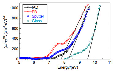
Figure 5.
The optical bandgaps of SiO2 films and silica
-
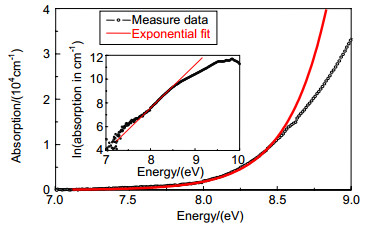
Figure 6.
The fit of Urbach tail for SiO2 film deposited with IAD
-
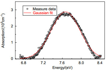
Figure 7.
The absorption and corresponding Guass fit of oxygen deficiency center in SiO2 films
-
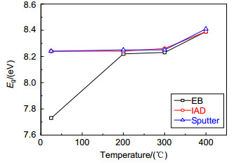
Figure 8.
The bandgaps of SiO2 films
-
Figure 9.
The Urbach tail energy of SiO2 films
-
Figure 10.
The content of oxygen-defect-center of SiO2 films


