
 E-mail Alert
 RSS
RSS
| Citation: |
Luo Zhijun, Liu Yanan, Chen Menglin, et al. Industrialization oriented technology of dual-beam super-resolution data storage[J]. Opto-Electronic Engineering, 2019, 46(3): 180559. doi: 10.12086/oee.2019.180559

|
Industrialization oriented technology of dual-beam super-resolution data storage
-
Abstract
Though optical data storage technology has attractive potential because of its long storage lifetime and low energy consumption, current optical data storage technologies are challenged by their capacity and dentistry for big data application. Dual-beam super-resolution optical data storage technology exhibits obvious advantage in ultra-high capacity and density due to the overcoming of optical diffraction limit. This work illuminates the key problems in the industrialization of dual-beam super-resolution optical data storage technology, and discusses some basic solutions to these obstacles. -

-
References
[1] Gan Z S, Cao Y Y, Evans R A, et al. Three-dimensional deep sub-diffraction optical beam lithography with 9 nm feature size[J]. Nature Communications, 2013, 4: 2061. doi: 10.1038/ncomms3061 [2] Rittweger E, Han K Y, Irvine S E, et al. STED microscopy reveals crystal colour centres with nanometric resolution[J]. Nature Photonics, 2009, 3(3): 144-147. doi: 10.1038/nphoton.2009.2 [3] Li L J, Gattass R R, Gershgoren E, et al. Achieving λ/20 resolution by one-color initiation and deactivation of polymerization[J]. Science, 2009, 324(5929): 910-913. doi: 10.1126/science.1168996 [4] Andrew T L, Tsai H Y, Menon R. Confining light to deep subwavelength dimensions to enable optical nanopatterning[J]. Science, 2009, 324(5929): 917-921. doi: 10.1126/science.1167704 [5] Scott T F, Kowalski B A, Sullivan A C, et al. Two-color single-photon photoinitiation and photoinhibition for subdiffraction photolithography[J]. Science, 2009, 324(5929): 913-917. doi: 10.1126/science.1167610 [6] Stocker M P, Li L J, Gattass R R, et al. Multiphoton photoresists giving nanoscale resolution that is inversely dependent on exposure time[J]. Nature Chemistry, 2011, 3(3): 223-227. doi: 10.1038/nchem.965 [7] Cao Y Y, Gan Z S, Jia B H, et al. High-photosensitive resin for super-resolution direct-laser-writing based on photoinhibited polymerization[J]. Optics Express, 2011, 19(20): 19486-19494. doi: 10.1364/OE.19.019486 [8] Fischer J, Von Freymann G, Wegener M. The materials challenge in diffraction-unlimited direct-laser-writing optical lithography[J]. Advanced Materials, 2010, 22(32): 3578-3582. doi: 10.1002/adma.201000892 [9] Harke B, Dallari W, Grancini G, et al. Polymerization inhibition by triplet state absorption for nanoscale lithography[J]. Advanced Materials, 2013, 25(6): 904-909. doi: 10.1002/adma.v25.6 [10] Wollhofen R, Katzmann J, Hrelescu C, et al. 120 nm resolution and 55 nm structure size in STED-lithography[J]. Optics Express, 2013, 21(9): 10831-10840. doi: 10.1364/OE.21.010831 [11] 刘铁诚, 张力, 孙静, 等.二芳基乙烯的光学性质及其在超分辨光存储中的应用[J].中国激光, 2018, 45(9): 0903001. Liu T C, Zhang L, Sun J, et al. Optical properties of dithienylethene and its applications in super-resolution optical storage[J]. Chinese Journal of Lasers, 2018, 45(9): 0903001. [12] Göttfert F, Wurm C A, Mueller V, et al. Coaligned dual-channel STED nanoscopy and molecular diffusion analysis at 20 nm resolution[J]. Biophysical Journal, 2013, 105(1): L01-L03. doi: 10.1016/j.bpj.2013.05.029 [13] Hell S, Jakobs S, Andresen M, et al. Method and apparatus for storing a three-dimensional arrangement of data bits in a solid-state body: 20070047287[P]. 2007-03-01. [14] Polyakova S M, Belov V N, Bossi M L, et al. Synthesis of photochromic compounds for aqueous solutions and focusable light[J]. European Journal of Organic Chemistry, 2011, 2011(18): 3301-3312. doi: 10.1002/ejoc.201100166 [15] Gan Z S, Evans R A, Gu M. Far-field super-resolution recording and reading towards petabyte optical discs[C]//Frontiers in Optics 2016, Rochester, New York United States, 2016. [16] Hell S W, Wichmann J. Breaking the diffraction resolution limit by stimulated emission: stimulated-emission-depletion fluorescence microscopy[J]. Optics Letters, 1994, 19(11): 780-782. doi: 10.1364/OL.19.000780 [17] Nielson R, Kaehr B, Shear J B. Microreplication and design of biological architectures using dynamic‐mask multiphoton lithography[J]. Small, 2009, 5(1): 120-125. doi: 10.1002/smll.v5:1 -
Overview

Overview: Compared with the hard drive disk and solid state disk, longer storage lifetime and lower energy consumption data storage is required for Big Data centers. Optical data storage has the advantage of these two characteristics, but for traditional optical discs, such as blue-ray discs, their storage capacity is limited because of optical diffraction. Ultra high density optical storage has been extensively studied in recent years for its potential application for Big Data centers. Dual-beam super-resolution optical data storage has the potential to achieve petabyte capacity for a single standard disc by overcoming the optical diffraction limit. This dual-beam super-resolution storage technology combines technologies of dual-beam super-resolution laser nanofabrication and stimulated emission depletion (STED) microscopy. Dual-beam super-resolution laser nanofabrication can realize 9 nm feature size and about 50 nm feature resolution. STED microscopy has obtained a best resolution 5.8 nm at the current state of the art. Dual beam super-resolution optical data storage employees two lasers. One has a Gaussian shape of its focus plane, and the other is focused as a doughnut shape with zero intensity at the center. The doughnut shaped beam depletes the effect of Gaussian shaped laser interacting with materials in the processes of data recording and readout to acquire a resolution beyond the optical diffraction limit. For industrialization of dual-beam super-resolution optical data storage, we illuminate the key problems of storage medium, super-resolution data recording, super-resolution data readout and super-resolution positioning. The storage medium should be a solid film after disc fabrication, and have material property change such as fluorescence intensity enhancement induced by local illumination of the Gaussian shape laser to enable data recording and readout. The storage medium should be specifically designed to be capable of adopting the dual-beam approach to realize super-resolution. Except super-resolution recording and readout, super-resolution positioning technology is also required to guarantee position accurate data manipulation at the nanoscale. We propose a STED microscopy approach for super-resolution positioning in the super-resolution optical data storage setup. To simplify the optical system integration with a best achievable stability, separated super-resolution optical data recording and readout setup is suggested. The method to speed up data recording and readout is also discussed.
-
Access History


Export File
Citation
Luo Zhijun, Liu Yanan, Chen Menglin, et al. Industrialization oriented technology of dual-beam super-resolution data storage[J]. Opto-Electronic Engineering, 2019, 46(3): 180559. doi: 10.12086/oee.2019.180559
Format
Content
 DownLoad:
-
Figure 1.
Schematic of stimulated emission depletion microscopy. (a) Electronic transition; (b) Intensity overlap of dual-beam and the effective excitation laser; (c) Feature size of dual-beam and effective excitation laser on focal plane; (d) Super-resolution photoinduction-inhibition nanolithography
-
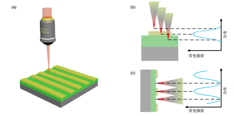
Figure 2.
(a) Dual-beam super-resolution scanning disc surface; (b) Fluorescent axial positioning servo; (c) Fluorescent radial positioning servo


