
 E-mail Alert
 RSS
RSS
| Citation: |
Chen R, Wang J C, Zhang W Z, et al. Research progress of laser manufacturing technology for microstructure sensor[J]. Opto-Electron Eng, 2023, 50(3): 220041. doi: 10.12086/oee.2023.220041

|
Research progress of laser manufacturing technology for microstructure sensor
-
Abstract
Microstructure sensor is a sensor device with the micro-scale structure as a sensitive unit and can convert external physical, chemical, and biological signals into electrical signals. It has been widely used in intelligent robots, health monitoring, virtual electronics, and other fields. At present, the manufacturing methods of microstructure sensors mainly include laser manufacturing technology, MEMS technology, and 3D printing technology. Laser manufacturing technology is a green processing method that focuses the high-energy laser beam on the object to be processed and makes the laser interact with the material, mainly including laser ablation, laser direct writing, laser induction, and laser-template composite processing. It has the advantages of non-contact processing, no mask, and customizable manufacturing. By optimizing the parameters of the laser manufacturing process, it can realize the efficient and low-cost manufacturing of microstructures with different sizes and shapes. In this paper, the types, function, and manufacturing technology of the microstructures are summarized. At the same time, the microstructure sensors fabricated by laser manufacturing technology are summarized and classified, and the manufacturing technology and application of bioelectric sensors, temperature sensors and pressure sensors are analyzed in detail. Finally, the development trends of the laser manufacturing technology for microstructure sensors are summarized and prospected.-
Keywords:
- laser manufacturing /
- microstructure /
- bioelectric sensors /
- temperature sensors /
- pressure sensors
-

-
References
[1] Ruth S R A, Feig V R, Tran H, et al. Microengineering pressure sensor active layers for improved performance[J]. Adv Funct Mater, 2020, 30(39): 2003491. doi: 10.1002/adfm.202003491 [2] Satti A T, Park J, Park J, et al. Fabrication of parylene-coated microneedle array electrode for wearable ECG device[J]. Sensors, 2020, 20(18): 5183. doi: 10.3390/s20185183 [3] Jiang H, Zhang X, Gu W, et al. Synthesis of ZnO particles with multi-layer and biomorphic porous microstructures and ZnO/rGO composites and their applications for photocatalysis[J]. Chem Phys Lett, 2018, 711: 100−106. doi: 10.1016/j.cplett.2018.08.013 [4] Chao M Y, Wang Y G, Ma D, et al. Wearable MXene nanocomposites-based strain sensor with tile-like stacked hierarchical microstructure for broad-range ultrasensitive sensing[J]. Nano Energy, 2020, 78: 105187. doi: 10.1016/j.nanoen.2020.105187 [5] Schwartz G, Tee B C K, Mei J G, et al. Flexible polymer transistors with high pressure sensitivity for application in electronic skin and health monitoring[J]. Nat Commun, 2013, 4: 1859. doi: 10.1038/ncomms2832 [6] Billard A, Kragic D. Trends and challenges in robot manipulation[J]. Science, 2019, 364(6446): eaat8414. doi: 10.1126/science.aat8414 [7] Yang J C, Mun J, Kwon S Y, et al. Electronic skin: recent progress and future prospects for skin-attachable devices for health monitoring, robotics, and prosthetics[J]. Adv Mater, 2019, 31(48): 1904765. doi: 10.1002/adma.201904765 [8] Tran A V, Zhang X M, Zhu B L. The development of a new piezoresistive pressure sensor for low pressures[J]. IEEE Trans Ind Electron, 2018, 65(8): 6487−6496. doi: 10.1109/TIE.2017.2784341 [9] Li J, Bao R R, Tao J, et al. Recent progress in flexible pressure sensor arrays: from design to applications[J]. J Mater Chem C, 2018, 6(44): 11878−11892. doi: 10.1039/C8TC02946F [10] Tachi S, Tsujimoto K, Okudaira S. Low-temperature reactive ion etching and microwave plasma etching of silicon[J]. Appl Phys Lett, 1988, 52(8): 616−618. doi: 10.1063/1.99382 [11] Kong J, Cassell A M, Dai H J. Chemical vapor deposition of methane for single-walled carbon nanotubes[J]. Chem Phys Lett, 1998, 292(4–6): 567−574. doi: 10.1016/S0009-2614(98)00745-3 [12] Martin C R, Van Dyke L S, Cai Z H, et al. Template synthesis of organic microtubules[J]. J Am Chem Soc, 1990, 112(24): 8976−8977. doi: 10.1021/ja00180a050 [13] Whitesides G M, Grzybowski B. Self-assembly at all scales[J]. Science, 2002, 295(5564): 2418−2421. doi: 10.1126/science.1070821 [14] Chou S Y, Krauss P R, Renstrom P J. Nanoimprint lithography[J]. J Vac Sci Technol B Microelectron Nanometer Struct Process Meas Phenom, 1996, 14(6): 4129−4133. doi: 10.1116/1.588605 [15] Xia Y N, Whitesides G M. Soft lithography[J]. Annu Rev Mater Sci, 1998, 28(1): 153−184. doi: 10.1146/annurev.matsci.28.1.153 [16] Yong J L, Yang Q, Guo C L, et al. A review of femtosecond laser-structured superhydrophobic or underwater superoleophobic porous surfaces/materials for efficient oil/water separation[J]. RSC Adv, 2019, 9(22): 12470−12495. doi: 10.1039/C8RA10673H [17] Zhang C Y, Zhou W, Geng D, et al. Laser direct writing and characterizations of flexible piezoresistive sensors with microstructures[J]. Opto-Electron Adv, 2021, 4(4): 04200061. doi: 10.29026/oea.2021.200061 [18] 张嘉琪, 高阳, 李淳, 等. 基于激光直写的柔性天线传感器研究[J]. 光电工程, 2022, 49(1): 210316. doi: 10.12086/oee.2022.210316 Zhang J Q, Gao Y, Li C, et al. Laser direct writing of flexible antenna sensor for strain and humidity sensing[J]. Opto-Electron Eng, 2022, 49(1): 210316. doi: 10.12086/oee.2022.210316 [19] 汪延成, 刘佳薇, 盘何旻, 等. 聚合物基表面微结构的逐面式制造技术研究进展[J]. 机械工程学报, 2021, 57(21): 220−233. doi: 10.3901/JME.2021.21.220 Wang Y C, Liu J W, Pan H M, et al. Recent progress on manufacturing technologies in layer-by-layer mode for the fabrication of polymer-based surface microstructures[J]. J Mech Eng, 2021, 57(21): 220−233. doi: 10.3901/JME.2021.21.220 [20] Tran K T M, Gavitt T D, Farrell N J, et al. Transdermal microneedles for the programmable burst release of multiple vaccine payloads[J]. Nat Biomed Eng, 2021, 5(9): 998−1007. doi: 10.1038/s41551-020-00650-4 [21] 周伟, 刘伟, 邱清富, 等. 生物医用电极制造技术及应用研究进展[J]. 科学通报, 2015, 60(15): 1352−1360. doi: 10.1360/N972014-01093 Zhou W, Liu W, Qiu Q F, et al. Development, fabrication, and applications of biomedical electrodes[J]. Chin Sci Bull, 2015, 60(15): 1352−1360. doi: 10.1360/N972014-01093 [22] 史杨, 许兵, 吴东, 等. 飞秒激光直写技术制备功能化微流控芯片研究进展[J]. 中国激光, 2019, 46(10): 1000001. doi: 10.3788/CJL201946.1000001 Shi Y, Xu B, Wu D, et al. Research progress on fabrication of functional microfluidic chips using femtosecond laser direct writing technology[J]. Chin J Lasers, 2019, 46(10): 1000001. doi: 10.3788/CJL201946.1000001 [23] Cao Y, Yuan X W, Wang X, et al. Synthesis and controlled release kinetics of pH-sensitive hollow polyaniline microspheres encapsuled with the corrosion inhibitor[J]. J Mol Liq, 2021, 342: 117497. doi: 10.1016/j.molliq.2021.117497 [24] Tang X, Wu C Y, Gan L, et al. Multilevel microstructured flexible pressure sensors with ultrahigh sensitivity and ultrawide pressure range for versatile electronic skins[J]. Small, 2019, 15(10): 1804559. doi: 10.1002/smll.201804559 [25] 肖靖吁. 新型可穿戴式生物传感器的构建及其对汗液分析的研究[D]. 北京: 北京科技大学, 2022. Xiao J Y. Construction of novel wearable biosensors and their researches on sweat analysis[D]. Beijing: University of Science and Technology Beijing, 2022. [26] Xu G, Cheng C, Liu Z Y, et al. Battery-free and wireless epidermal electrochemical system with all-printed stretchable electrode array for multiplexed In situ sweat analysis[J]. Adv Mater Technol, 2019, 4(7): 1800658. doi: 10.1002/admt.201800658 [27] Xu K C, Zhou R, Takei K, et al. Toward flexible surface-enhanced Raman scattering (SERS) sensors for point-of-care diagnostics[J]. Adv Sci, 2019, 6(16): 1900925. doi: 10.1002/advs.201900925 [28] Wu R H, Ma L Y, Hou C, et al. Silk composite electronic textile sensor for high space precision 2D combo temperature–pressure sensing[J]. Small, 2019, 15(31): 1901558. doi: 10.1002/smll.201901558 [29] Wang Y, Yang L, Shi X L, et al. Flexible thermoelectric materials and generators: challenges and innovations[J]. Adv Mater, 2019, 31(29): 1807916. doi: 10.1002/adma.201807916 [30] Park K C, Choi H J, Chang C H, et al. Nanotextured silica surfaces with robust superhydrophobicity and omnidirectional broadband supertransmissivity[J]. ACS Nano, 2012, 6(5): 3789−3799. doi: 10.1021/nn301112t [31] Cai J X, Zhang C P, Liang C W, et al. Solution-processed large-area gold nanocheckerboard metasurfaces on flexible plastics for plasmonic biomolecular sensing[J]. Adv Opt Mater, 2019, 7(19): 1900516. doi: 10.1002/adom.201900516 [32] Chen L W, Zhou Y, Wu M X, et al. Remote-mode microsphere nano-imaging: new boundaries for optical microscopes[J]. Opto-Electron Adv, 2018, 1(1): 170001. doi: 10.29026/oea.2018.170001 [33] Esmann M, Lamberti F R, Harouri A, et al. Brillouin scattering in hybrid optophononic Bragg micropillar resonators at 300 GHz[J]. Optica, 2019, 6(7): 854−859. doi: 10.1364/OPTICA.6.000854 [34] 廖嘉宁, 张东石, 李铸国. 飞秒激光制备柔性电子器件进展[J]. 光电工程, 2022, 49(2): 210388. doi: 10.12086/oee.2022.210388 Liao J N, Zhang D S, Li Z G. Advance in femtosecond laser fabrication of flexible electronics[J]. Opto-Electron Eng, 2022, 49(2): 210388. doi: 10.12086/oee.2022.210388 [35] Jiang H B, Zhang Y L, Liu Y, et al. Bioinspired few-layer graphene prepared by chemical vapor deposition on femtosecond laser-structured Cu foil[J]. Laser Photonics Rev, 2016, 10(3): 441−450. doi: 10.1002/lpor.201500256 [36] Zhou W, Liu W, Liu S Y, et al. Experimental investigation on surface wettability of copper-based dry bioelectrodes[J]. Sensors Actuat A Phys, 2016, 244: 237−242. doi: 10.1016/j.sna.2016.04.044 [37] Yong J L, Yang Q, Chen F, et al. Stable superhydrophobic surface with hierarchical mesh-porous structure fabricated by a femtosecond laser[J]. Appl Phys A, 2013, 111(1): 243−249. doi: 10.1007/s00339-013-7572-z [38] Crawford T H R, Borowiec A, Haugen H K. Femtosecond laser micromachining of grooves in silicon with 800 nm pulses[J]. Appl Phys A, 2005, 80(8): 1717−1724. doi: 10.1007/s00339-004-2941-2 [39] Li G Q, Fan H, Ren F F, et al. Multifunctional ultrathin aluminum foil: oil/water separation and particle filtration[J]. J Mater Chem A, 2016, 4(48): 18832−18840. doi: 10.1039/C6TA08231A [40] Yan S G, Ren F F, Li C Z, et al. Unidirectional self-transport of air bubble via a Janus membrane in aqueous environment[J]. Appl Phys Lett, 2018, 113(26): 261602. doi: 10.1063/1.5052566 [41] Chen C, Huang Z C, Jiao Y L, et al. In situ reversible control between sliding and pinning for diverse liquids under ultra-low voltage[J]. ACS Nano, 2019, 13(5): 5742−5752. doi: 10.1021/acsnano.9b01180 [42] Lu Y, Yu L D, Zhang Z, et al. Biomimetic surfaces with anisotropic sliding wetting by energy-modulation femtosecond laser irradiation for enhanced water collection[J]. RSC Adv, 2017, 7(18): 11170−11179. doi: 10.1039/C6RA28174E [43] Han S, Hong S, Ham J, et al. Fast plasmonic laser nanowelding for a Cu-nanowire percolation network for flexible transparent conductors and stretchable electronics[J]. Adv Mater, 2014, 26(33): 5808−5814. doi: 10.1002/adma.201400474 [44] 何宇豪. 基于SU8胶制备立体结构柔性压阻传感器及其性能研究[D]. 成都: 电子科技大学, 2019. He Y H. The fabrication and capability researches about flexible piezoresistive sensor based on SU8 photoresist[D]. Chengdu: University of Electronic Science and Technology of China, 2019. [45] Li J, Wu T Y, Jiang H, et al. Ultrasensitive hierarchical piezoresistive pressure sensor for wide-range pressure detection[J]. Adv Intell Syst, 2021, 3(11): 2100070. doi: 10.1002/aisy.202100070 [46] Wu Y, Ji L F, Lin Z Y, et al. Substrate effect of laser surface sub-micro patterning by means of self-assembly SiO2 microsphere array[J]. Appl Surf Sci, 2015, 357: 832−837. doi: 10.1016/j.apsusc.2015.09.066 [47] Fang Y, Yong J L, Chen F, et al. Bioinspired fabrication of bi/tridirectionally anisotropic sliding superhydrophobic PDMS surfaces by femtosecond laser[J]. Adv Mater Interfaces, 2018, 5(6): 1701245. doi: 10.1002/admi.201701245 [48] Yong J L, Yang Q, Huo J L, et al. Underwater gas self-transportation along femtosecond laser-written open superhydrophobic surface microchannels (< 100 µm) for bubble/gas manipulation[J]. Int J Extreme Manuf, 2022, 4(1): 015002. doi: 10.1088/2631-7990/ac466f [49] Li M J, Yang Q, Chen F, et al. Integration of great water repellence and imaging performance on a superhydrophobic PDMS microlens array by femtosecond laser microfabrication[J]. Adv Eng Mater, 2019, 21(3): 1800994. doi: 10.1002/adem.201800994 [50] Tian H, Shu Y, Wang X F, et al. A graphene-based resistive pressure sensor with record-high sensitivity in a wide pressure range[J]. Sci Rep, 2015, 5: 8603. doi: 10.1038/srep08603 [51] Chen R, Luo T, Geng D, et al. Facile fabrication of a fast-response flexible temperature sensor via laser reduced graphene oxide for contactless human-machine interface[J]. Carbon, 2022, 187: 35−46. doi: 10.1016/j.carbon.2021.10.064 [52] Zhu Y S, Cai H B, Ding H Y, et al. Fabrication of low-cost and highly sensitive graphene-based pressure sensors by direct laser scribing polydimethylsiloxane[J]. ACS Appl Mater Interfaces, 2019, 11(6): 6195−6200. doi: 10.1021/acsami.8b17085 [53] He M H, Wang Y N, Wang S R, et al. Laser-induced graphene enabled 1D fiber electronics[J]. Carbon, 2020, 168: 308−318. doi: 10.1016/j.carbon.2020.06.084 [54] Kim E, Lee Y, Ko C, et al. Tuning the optical and electrical properties of MoS2 by selective Ag photo-reduction[J]. Appl Phys Lett, 2018, 113(1): 013105. doi: 10.1063/1.5022705 [55] Szustakiewicz K, Stępak B, Antończak A, et al. Femtosecond laser-induced modification of PLLA/hydroxyapatite composite[J]. Polym Degrad Stab, 2018, 149: 152−161. doi: 10.1016/j.polymdegradstab.2018.01.015 [56] Fathi-Hafshejani P, Johnson H, Ahmadi Z, et al. Phase-selective and localized TiO2 coating on additive and wrought titanium by a direct laser surface modification approach[J]. ACS Omega, 2020, 5(27): 16744−16751. doi: 10.1021/acsomega.0c01671 [57] Yeo J, Hong S, Kim G, et al. Laser-induced hydrothermal growth of heterogeneous metal-oxide nanowire on flexible substrate by laser absorption layer design[J]. ACS Nano, 2015, 9(6): 6059−6068. doi: 10.1021/acsnano.5b01125 [58] Palaniappan V, Masihi S, Panahi M, et al. Laser-assisted fabrication of flexible micro-structured pressure sensor for low pressure applications[C]//2019 IEEE International Conference on Flexible and Printable Sensors and Systems (FLEPS), 2019: 1–3. [59] Rana A, Roberge J P, Duchaine V. An improved soft dielectric for a highly sensitive capacitive tactile sensor[J]. IEEE Sens J, 2016, 16(22): 7853−7863. doi: 10.1109/JSEN.2016.2605134 [60] Dos Santos A, Pinela N, Alves P, et al. Piezoresistive E-skin sensors produced with laser engraved molds[J]. Adv Electron Mater, 2018, 4(9): 1800182. doi: 10.1002/aelm.201800182 [61] Dos Santos A, Pinela N, Alves P, et al. E-skin bimodal sensors for robotics and prosthesis using PDMS molds engraved by laser[J]. Sensors, 2019, 19(4): 899. doi: 10.3390/s19040899 [62] Li Z Y, Zhang B, Li K, et al. A wide linearity range and high sensitivity flexible pressure sensor with hierarchical microstructures via laser marking[J]. J Mater Chem C, 2020, 8(9): 3088−3096. doi: 10.1039/C9TC06352H [63] Su Y, Zhang W, Chen S M, et al. Piezoresistive electronic-skin sensors produced with self-channeling laser microstructured silicon molds[J]. IEEE Trans Electron Devices, 2021, 68(2): 786−792. doi: 10.1109/TED.2020.3045962 [64] Kam D H, Kim J, Mazumder J. Near-IR nanosecond laser direct writing of multi-depth microchannel branching networks on silicon[J]. J Manuf Process, 2018, 35: 99−106. doi: 10.1016/j.jmapro.2018.07.023 [65] Xu F L, Li X Y, Shi Y, et al. Recent developments for flexible pressure sensors: a review[J]. Micromachines, 2018, 9(11): 580. doi: 10.3390/mi9110580 [66] Geng D, Chen S Y, Chen R, et al. Tunable wide range and high sensitivity flexible pressure sensors with ordered multilevel microstructures[J]. Adv Mater Technol, 2022, 7(6): 2101031. doi: 10.1002/admt.202101031 [67] Gao Y, Lu C, Yu G H, et al. Laser micro-structured pressure sensor with modulated sensitivity for electronic skins[J]. Nanotechnology, 2019, 30(32): 325502. doi: 10.1088/1361-6528/ab1a86 [68] Archard J F. Elastic deformation and the laws of friction[J]. Proc Roy Soc A Math Phys Sci, 1957, 243(1233): 190−205. doi: 10.1098/rspa.1957.0214 [69] Schallamach A. The load dependence of rubber friction[J]. Proc Phys Soc B, 1952, 65(9): 657−661. doi: 10.1088/0370-1301/65/9/301 [70] Shi J D, Wang L, Dai Z H, et al. Multiscale hierarchical design of a flexible piezoresistive pressure sensor with high sensitivity and wide linearity range[J]. Small, 2018, 14(27): 1800819. doi: 10.1002/smll.201800819 [71] Zhang C Y, Chen R, Xiao C Q, et al. Laser direct writing of highly ordered two-level hierarchical microstructures for flexible piezoresistive sensor with enhanced sensitivity[J]. Adv Mater Interfaces, 2022, 9(1): 2101596. doi: 10.1002/admi.202101596 [72] Du Q F, Liu L L, Tang R T, et al. High-performance flexible pressure sensor based on controllable hierarchical microstructures by laser scribing for wearable electronics[J]. Adv Mater Technol, 2021, 6(9): 2100122. doi: 10.1002/admt.202100122 [73] 朱芸松. 基于石墨烯的表皮压力传感器的设计、制备与建模[D]. 合肥: 中国科学技术大学, 2018. Zhu Y S. Design, fabrication and modeling of Graphene epidermal pressure sensor[D]. Hefei: University of Science and Technology of China, 2018. [74] Chen Z T, Zhao D N, Ma R, et al. Flexible temperature sensors based on carbon nanomaterials[J]. J Mater Chem B, 2021, 9(8): 1941−1964. doi: 10.1039/D0TB02451A [75] Gao W, Singh N, Song L, et al. Direct laser writing of micro-supercapacitors on hydrated graphite oxide films[J]. Nat Nanotechnol, 2011, 6(8): 496−500. doi: 10.1038/nnano.2011.110 [76] Romero FJ, Ortiz-Gomez I, Salinas A, et al. Temperature sensing by laser reduced graphene oxide at different laser power levels[C]//2020 IEEE Sensors, 2020: 1–5. [77] Kazemzadeh R, Kim W S. Flexible temperature sensor with laser scribed Graphene oxide[C]//14th IEEE International Conference on Nanotechnology, 2014: 420–423. [78] Jung H, Lee H. Semi-transparent reduced graphene oxide temperature sensor on organic light-emitting diodes for fingerprint liveness detection of smartphone authentication[J]. Sensors Actuat A Phys, 2021, 331: 112876. doi: 10.1016/j.sna.2021.112876 [79] Lin J, Peng Z W, Liu Y Y, et al. Laser-induced porous graphene films from commercial polymers[J]. Nat Commun, 2014, 5(1): 5714. doi: 10.1038/ncomms6714 [80] Wan Z F, Chen X, Gu M. Laser scribed graphene for supercapacitors[J]. Opto-Electron Adv, 2021, 4(7): 200079. doi: 10.29026/oea.2021.200079 [81] Chhetry A, Sharma S, Barman S C, et al. Black phosphorus@laser-engraved graphene heterostructure-based temperature-strain hybridized sensor for electronic-skin applications[J]. Adv Funct Mater, 2021, 31(10): 2007661. doi: 10.1002/adfm.202007661 [82] Lu Y Y, Fujita Y, Honda S, et al. Wireless and flexible skin moisture and temperature sensor sheets toward the study of thermoregulator center[J]. Adv Healthcare Mater, 2021, 10(17): 2100103. doi: 10.1002/adhm.202100103 [83] Nakajima T, Tsuchiya T. Ultrathin highly flexible featherweight ceramic temperature sensor arrays[J]. ACS Appl Mater Interfaces, 2020, 12(32): 36600−36608. doi: 10.1021/acsami.0c08718 [84] Le T S D, Park S, An J N, et al. Ultrafast laser pulses enable one-step graphene patterning on woods and leaves for green electronics[J]. Adv Funct Mater, 2019, 29(33): 1902771. doi: 10.1002/adfm.201902771 [85] Niu X, Gao X H, Liu Y F, et al. Surface bioelectric dry electrodes: a review[J]. Measurement, 2021, 183: 109774. doi: 10.1016/j.measurement.2021.109774 [86] Fu Y L, Zhao J J, Dong Y, et al. Dry electrodes for human bioelectrical signal monitoring[J]. Sensors, 2020, 20(13): 3651. doi: 10.3390/s20133651 [87] Baek J Y, Kang K M, Kim H J, et al. Manufacturing process of polymeric microneedle sensors for mass production[J]. Micromachines, 2021, 12(11): 1364. doi: 10.3390/mi12111364 [88] Mania G K, Ponnusamy D, Tsuchiya K. Ultrafast fabrication of microneedle array for transdermal Ion detection[C]//2018 International Symposium on Micro-NanoMechatronics and Human Science (MHS), 2018: 1–3. [89] Zhou W, Ling W S, Liu W, et al. Laser direct micromilling of copper-based bioelectrode with surface microstructure array[J]. Opt Lasers Eng, 2015, 73: 7−15. doi: 10.1016/j.optlaseng.2015.03.011 [90] Zhou W, Liu S Y, Liu W, et al. Novel dry metal electrode with tilted microstructure fabricated with laser micromilling process[J]. Sensors Actuat A Phys, 2017, 264: 76−83. doi: 10.1016/j.sna.2017.07.028 [91] Pearton M, Saller V, Coulman S A, et al. Microneedle delivery of plasmid DNA to living human skin: formulation coating, skin insertion and gene expression[J]. J Control Release, 2012, 160(3): 561−569. doi: 10.1016/j.jconrel.2012.04.005 [92] Sun Y W, Ren L, Jiang L L, et al. Fabrication of composite microneedle array electrode for temperature and bio-signal monitoring[J]. Sensors, 2018, 18(4): 1193. doi: 10.3390/s18041193 -
Overview
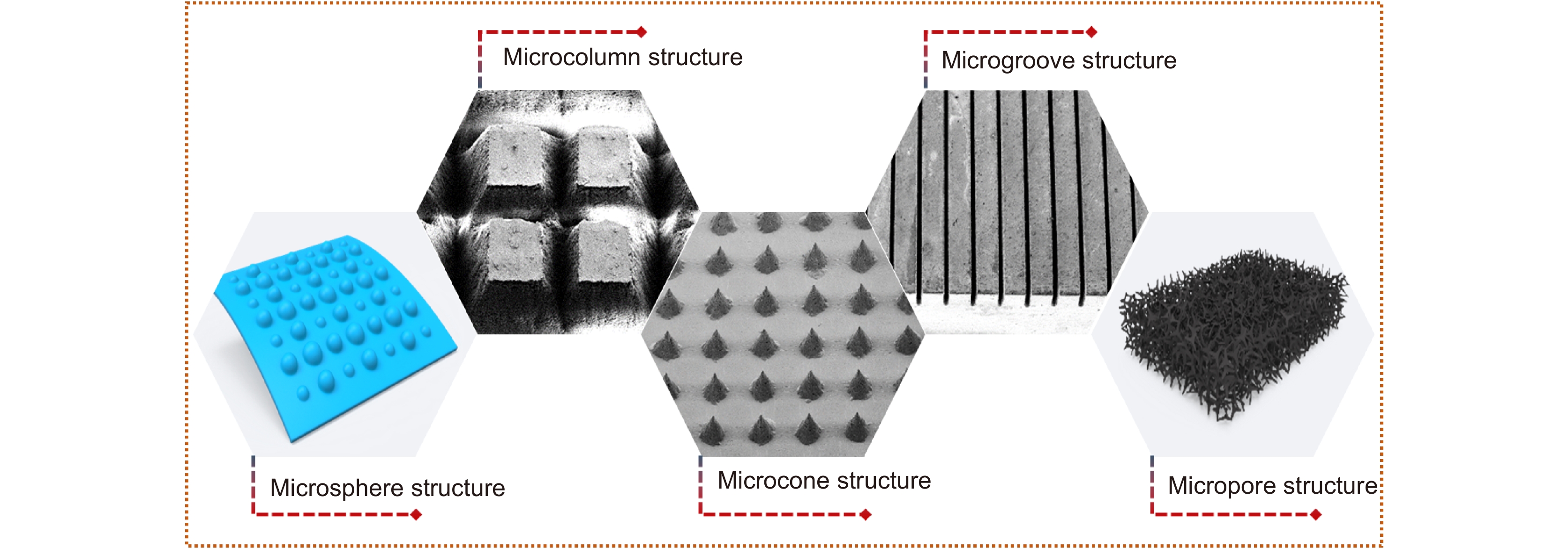
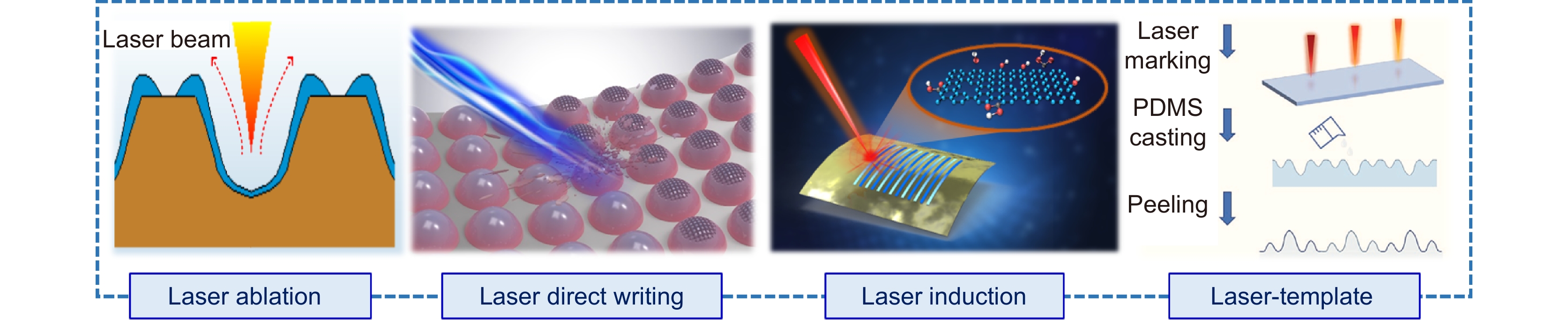
Microstructure sensor is a kind of sensor with a 2D or 3D micron-scale structure prepared by advanced manufacturing technology. It is used as a sensitive part to enhance the transmission characteristics of physical, chemical, and biological signals to the environment, and convert the external signals into electrical signals. The microstructure is generally a regular or disordered structure, usually in the shape of microspheres, microcolumns, microcones, microgrooves and micropores. The microstructures with different shapes can realize the functions of puncture, pressure transmission, vibration transmission, drug transmission, bioelectric transmission, heat transmission, sound transmission, gas adsorption, and so on. In recent years, researchers from all over the world have gradually attached great importance to the research on the manufacturing technology of microstructure sensors. At present, researchers have proposed the MEMS manufacturing processes, such as reactive ion etching and chemical vapor deposition, to achieve mass manufacturing of high-precision microstructures on flexible polymer materials and rigid materials. In addition, some researchers have also proposed the manufacturing processes such as template method, self-assembly, nanoimprinting, and soft lithography to realize microstructure manufacturing. However, the above-mentioned manufacturing processes usually cannot prepare microstructure in one step, which has the problems of complex process, high production cost, limited processing materials, and unable to control the microstructure morphology. In contrast, laser manufacturing technology has the advantages of non-contact processing, no mask, customizable manufacturing, etc. By optimizing the parameters of laser process (such as laser power, scanning speed, filling mode and scanning path), it can achieve efficient and low-cost manufacturing of microstructures with different sizes and shapes. Therefore, using laser manufacturing technology to realize microstructure manufacturing and applying it to bioelectricity, temperature, and pressure sensors has become a research hotspot in microstructure sensor manufacturing technology. Laser manufacturing technology mainly includes laser ablation, laser direct writing, laser induction, laser-template processing, etc. Laser ablation is an auxiliary heating process based on the thermochemical and thermophysical effects of a laser beam, which melts the materials to be processed to realize structural forming. Laser direct writing is a manufacturing process that focuses high-energy photon beams on the materials to be processed to produce a photochemical process, and manufacturing the structures through material removal. Laser-induced modification is a manufacturing process to change the physical and chemical properties of the materials to be processed. Laser-template processing is a manufacturing process that uses a laser to produce microstructure molds on silicon, glass, polymer, and other substrates, and then uses soft lithography technology to reverse die the structures on the molds. Based on the interaction between the laser and materials, the induction, removal, and migration of materials to be processed can be realized. By adjusting the laser processing mode and processing parameters, the controlled manufacturing of the 2D or 3D microstructures or the controlled preparation of functional materials for the sensitive units can be realized, breaking through the limitations of efficiency and cost of traditional manufacturing methods for microstructures. In this paper, the types, functions, and manufacturing technologies of microstructures are summarized and classified. The preparation processes of laser manufacturing technology and other advanced manufacturing technologies of microstructures are summarized. The applications of microstructure sensors prepared by laser ablation, laser direct writing, laser induction, and laser-template processing technology in bioelectric sensing, temperature sensing, and pressure sensing are described in detail. Finally, the development trend of the laser manufacturing technology for microstructure sensors is summarized and prospected.
-
Access History
Figures(8)
Tables(2)
Article Metrics

Export File
Citation
Chen R, Wang J C, Zhang W Z, et al. Research progress of laser manufacturing technology for microstructure sensor[J]. Opto-Electron Eng, 2023, 50(3): 220041. doi: 10.12086/oee.2023.220041
Format
Content
 DownLoad:
-
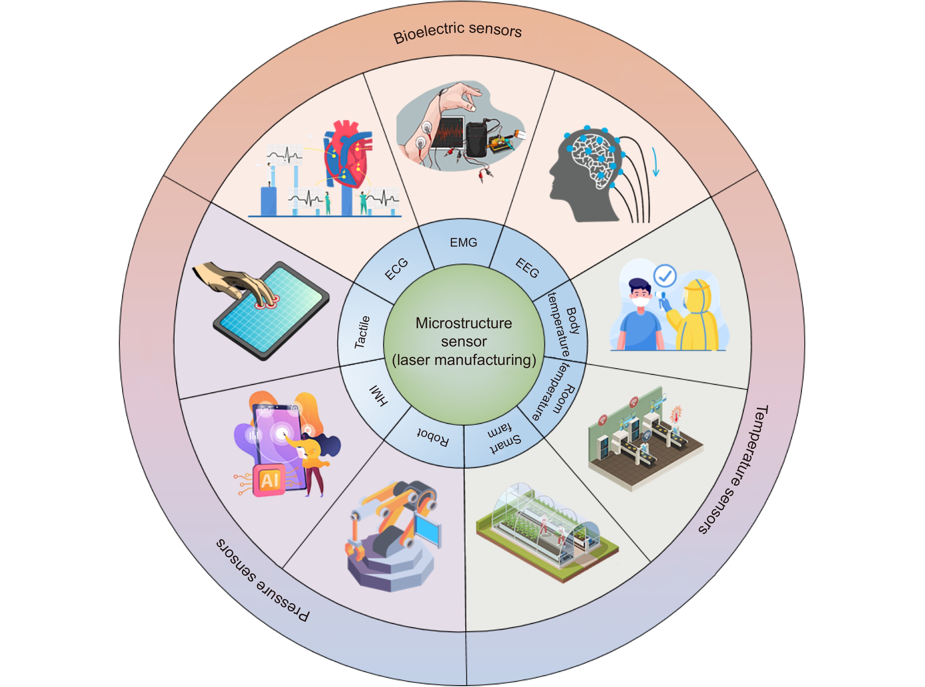
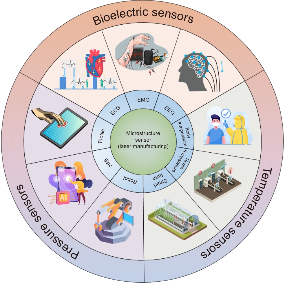
Figure 1.
Application of the microstructure sensor for bioelectricity, pressure and temperature detection
-
Figure 2.
Classification of microstructures
-
Figure 3.
Laser manufacturing method of microstructure
-
Figure 4.
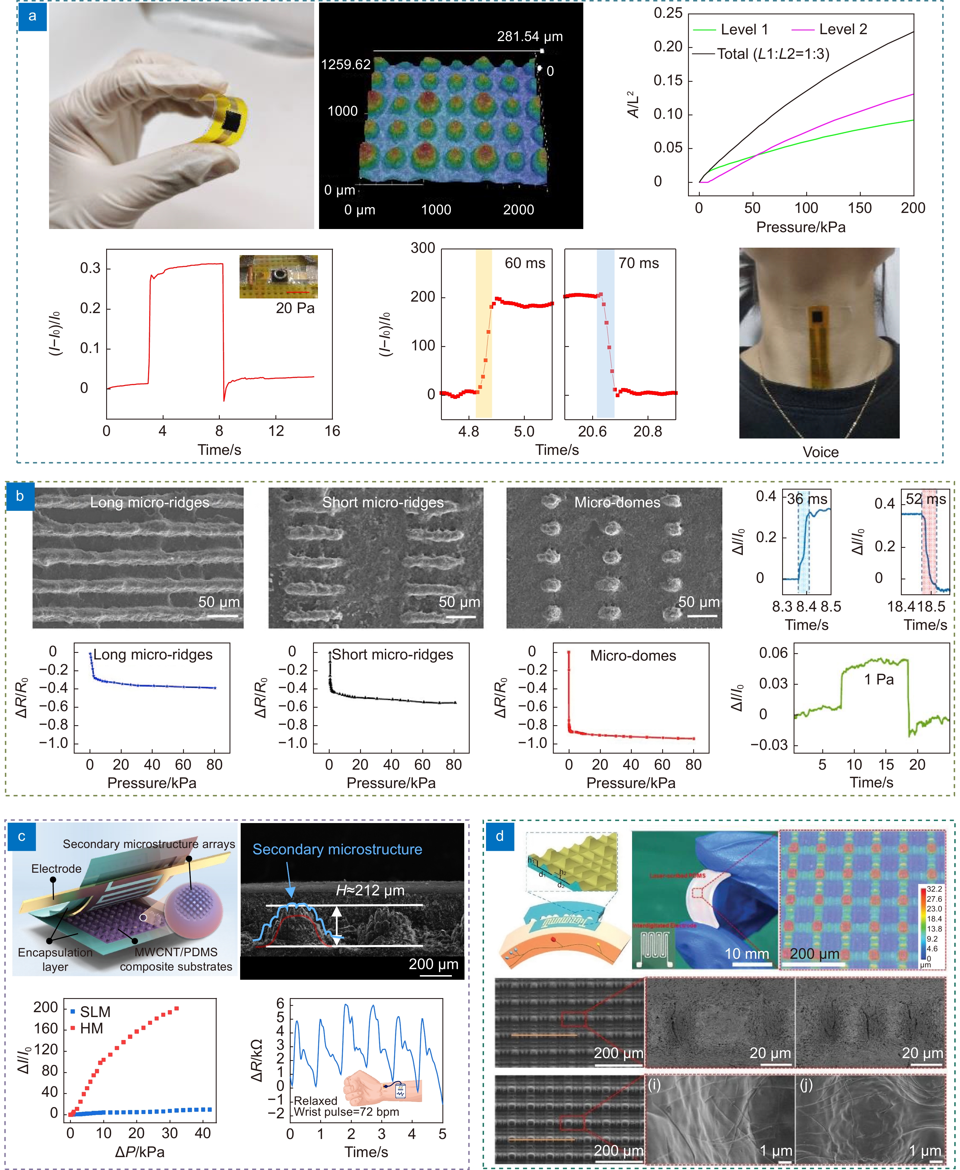
Laser manufacturing pressure sensor. (a) Image of the sensor and microstructure super-depth maps, response time testing, speech recognition applications[66]; (b) SEM images of three microstructures and performance test of sensors[67]; (c) Schematic diagram of microstructure sensor, SEM image, sensitivity and pulse performance test[71]; (d) Schematic diagram of sensor microstructure and SEM image[72]
-
Figure 5.
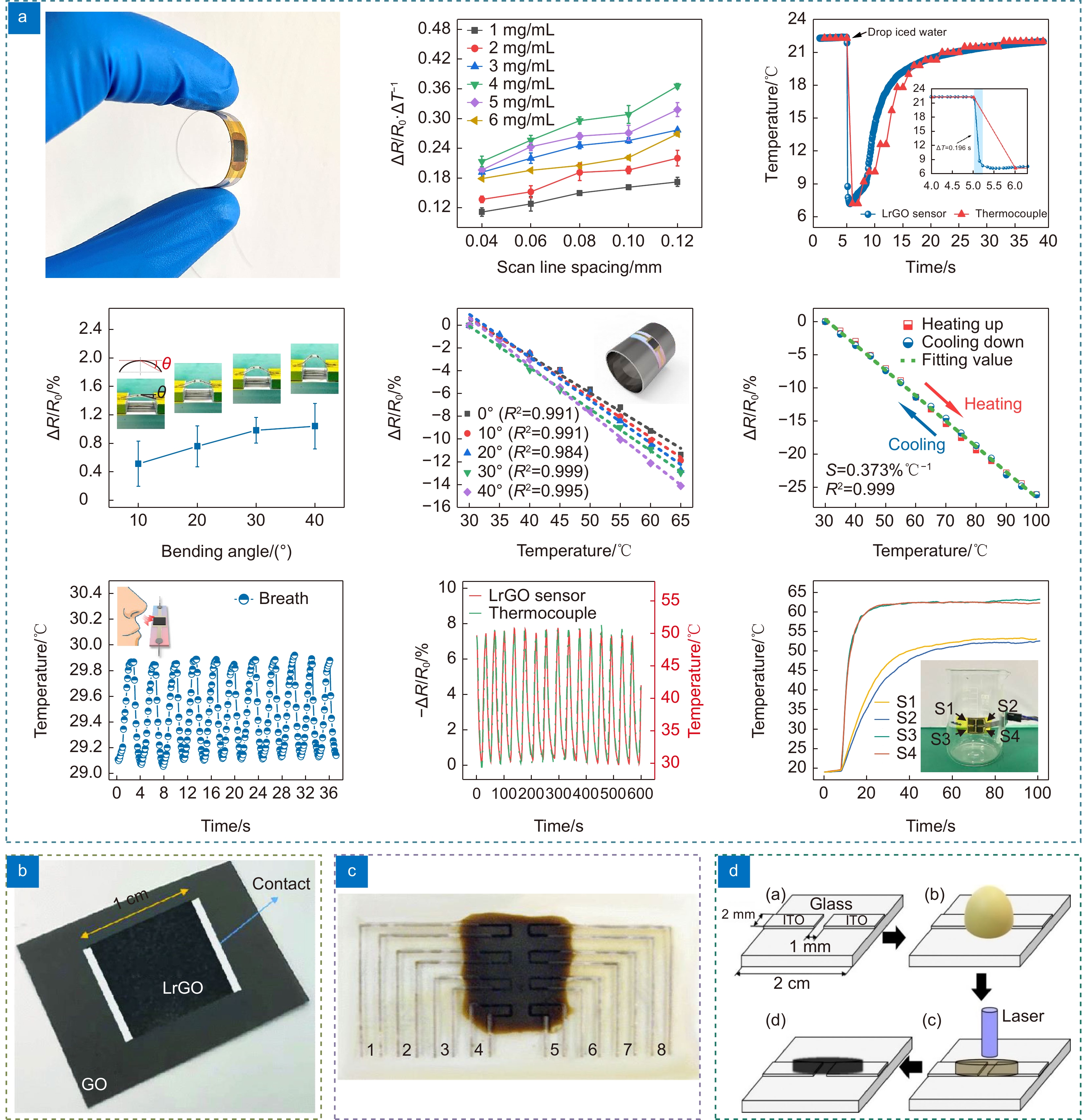
Temperature sensor based on the laser reduction of graphene oxide. (a) Image of the sensor, SEM image of the reduced graphene oxide, sensitivity, bending test hysteresis test, blowing and breathing performance test and curved surface test of the sensor[51]; (b) Laser reduced graphene oxide sensor diagram[76]; (c) Reduction of graphene oxide by laser[77]; (d) Sensor manfacturing process[78]
-
Figure 6.
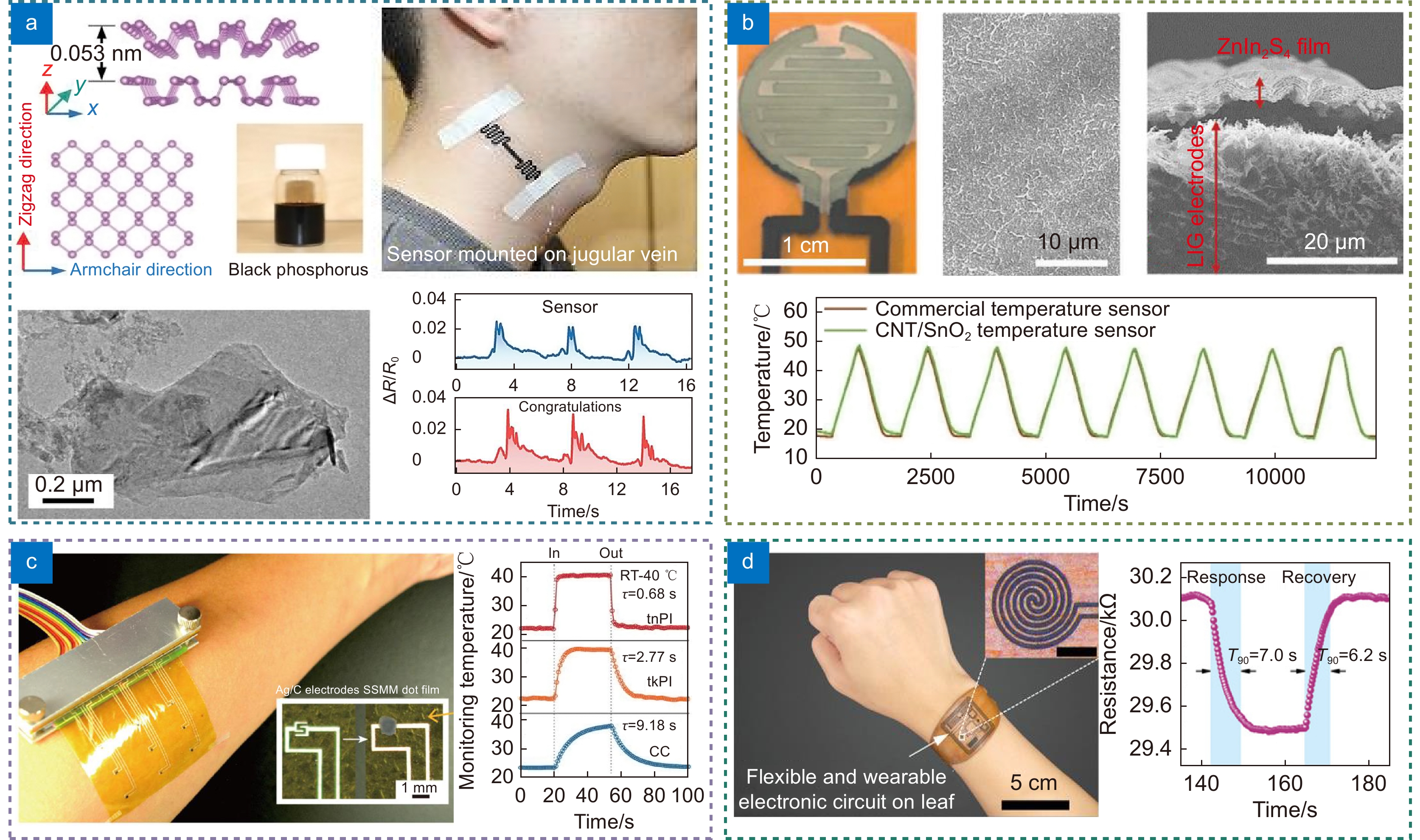
Temperature sensor based on the laser-induced graphene. (a) TEM image of the typical layered morphology of NMP-passivated BP nanosheet and Photograph illustrating location of sensor for jugular vein pulse measurement[81]; (b) Device photograph and SEM images of cross-sectional view of the ZIS nanosheets on porous graphene electrodes[82]; (c) Photograph of the 3 × 3 sensor and response curves for temperature monitoring[83]; (d) Leaf surface induced graphene patterning for temperature sensors[84]
-
Figure 7.
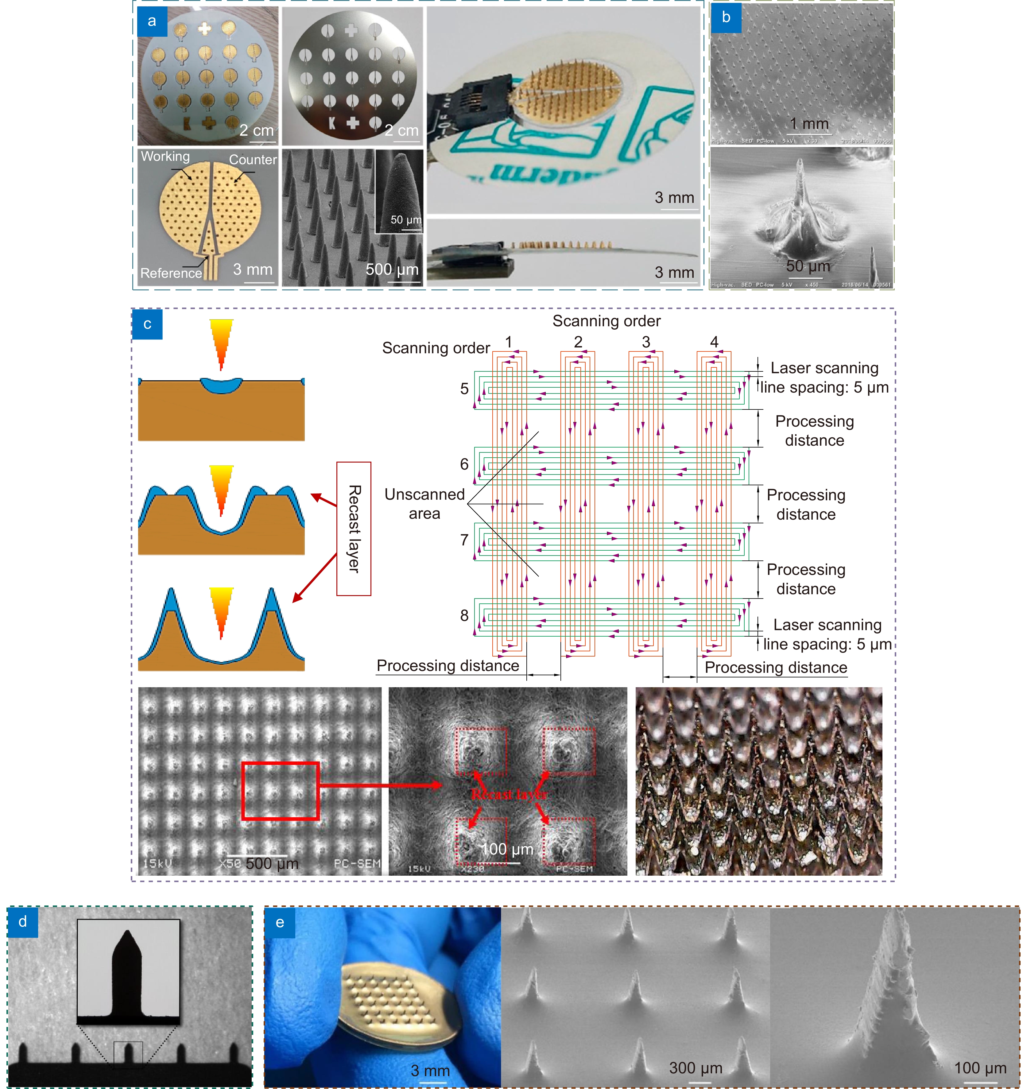
Microneedle Array Bioelectric Sensors. (a) SEM image of an array of microneedles on the sensor and top views of the microneedle sensor equipped with an adhesive film[87]; (b) Scanning electron microscope image of the PDMS microneedle before Au deposition[88]; (c) Dry electrode manufacturing process and SEM image of microneedle array[36, 89]; (d) Electrode optical image[91]; (e) Photograph of the sensor and SEM image of the microneedle[92]
- Figure .


