
 E-mail Alert
 RSS
RSS
| Citation: |
Jiang ZJ, Liu YJ, Wang L. Applications of optically and electrically driven nanoscale bowtie antennas. Opto-Electron Sci 1, 210004 (2022). doi: 10.29026/oes.2022.210004

|
Applications of optically and electrically driven nanoscale bowtie antennas
-
Abstract
Optical antennas play an important role in optical field manipulation. Among them, nanoscale bowtie antennas have been extensively studied for its high confinement and enhancement. In this mini-review, we start with a brief introduction of bowtie antennas and underlying physics. Then we review the applications with respect to optically and electrically excited nanoscale bowtie antennas. Optically driven bowtie antennas enable a set of optical applications such as near-field imaging/trapping, nonlinear response, nanolithography, photon generation and detection. Finally, we put emphasis on the principle and applications of electrically driven bowtie antennas, an emerging method of generating ultrafast and broadband tunable nanosources. In a word, nanoscale bowtie antennas still have great potential research value to explore.-
Keywords:
- bowtie antenna /
- near-field imaging /
- nanolithography /
- nonlinear /
- nanolaser /
- inelastic tunneling
-

-
References
[1] Synge EH. XXXVIII. A suggested method for extending microscopic resolution into the ultra-microscopic region. London, Edinburgh, Dublin Philos Mag J Sci 6, 356–362 (1928). doi: 10.1080/14786440808564615 [2] Bethe HA. Theory of diffraction by small holes. Phys Rev 66, 163–182 (1944). doi: 10.1103/PhysRev.66.163 [3] Wang L, Xu XF. High transmission nanoscale bowtie-shaped aperture probe for near-field optical imaging. Appl Phys Lett 90, 261105 (2007). doi: 10.1063/1.2752542 [4] Wang L, Uppuluri SM, Jin EX, Xu XF. Nanolithography using high transmission nanoscale bowtie apertures. Nano Lett 6, 361–364 (2006). doi: 10.1021/nl052371p [5] Balanis CA. Antenna Theory: Analysis and Design (Harper & Row, New York, 1982). [6] Grober RD, Schoelkopf RJ, Prober DE. Optical antenna: towards a unity efficiency near-field optical probe. Appl Phys Lett 70, 1354–1356 (1997). doi: 10.1063/1.118577 [7] Krasnok AE, Maksymov IS, Denisyuk AI, Belov PA, Miroshnichenko AE et al. Optical nanoantennas. Phys-Usp 56, 539–564 (2013). doi: 10.3367/UFNe.0183.201306a.0561 [8] Bharadwaj P, Deutsch B, Novotny L. Optical antennas. Adv Opt Photonics 1, 438–483 (2009). doi: 10.1364/AOP.1.000438 [9] Park J, Pasupathy AN, Goldsmith JI, Chang C, Yaish Y et al. Coulomb blockade and the Kondo effect in single-atom transistors. Nature 417, 722–725 (2002). doi: 10.1038/nature00791 [10] Huang JS, Kern J, Geisler P, Weinmann P, Kamp M et al. Mode imaging and selection in strongly coupled nanoantennas. Nano Lett 10, 2105–2110 (2010). doi: 10.1021/nl100614p [11] Sun HT, Liu XS, Su YJ, Deng B, Peng HL et al. Dirac-cone induced gating enhancement in single-molecule field-effect transistors. Nanoscale 11, 13117–13125 (2019). doi: 10.1039/C9NR01551E [12] Sun HT, Jiang ZL, Xin N, Guo XF, Hou SM et al. Efficient fabrication of stable graphene-molecule-graphene single-molecule junctions at room temperature. Chemphyschem 19, 2258–2265 (2018). doi: 10.1002/cphc.201800220 [13] Şendur K, Challener W. Near-field radiation of bow-tie antennas and apertures at optical frequencies. J Microsc 210, 279–283 (2003). doi: 10.1046/j.1365-2818.2003.01145.x [14] Jin EX, Xu XF. Obtaining super resolution light spot using surface plasmon assisted sharp ridge nanoaperture. Appl Phys Lett 86, 111106 (2005). doi: 10.1063/1.1875747 [15] Schuck PJ, Fromm DP, Sundaramurthy A, Kino GS, Moerner WE. Improving the mismatch between light and nanoscale objects with gold bowtie nanoantennas. Phys Rev Lett 94, 017402 (2005). doi: 10.1103/PhysRevLett.94.017402 [16] Sundaramurthy A, Schuck PJ, Conley NR, Fromm DP, Kino GS et al. Toward nanometer-scale optical photolithography: utilizing the near-field of bowtie optical nanoantennas. Nano Lett 6, 355–360 (2006). doi: 10.1021/nl052322c [17] Suh JY, Kim CH, Zhou W, Huntington MD, Co DT et al. Plasmonic bowtie nanolaser arrays. Nano Lett 12, 5769–5774 (2012). doi: 10.1021/nl303086r [18] Venuthurumilli PK, Ye PD, Xu XF. Plasmonic resonance enhanced polarization-sensitive photodetection by black phosphorus in near infrared. ACS Nano 12, 4861–4867 (2018). doi: 10.1021/acsnano.8b01660 [19] Qin J, Liu YJ, Luo HW, Jiang ZJ, Cai WS et al. Tunable light emission by electrically excited plasmonic antenna. ACS Photonics 6, 2392–2396 (2019). doi: 10.1021/acsphotonics.9b00954 [20] Dodson S, Haggui M, Bachelot R, Plain J, Li SZ et al. Optimizing electromagnetic hotspots in plasmonic bowtie nanoantennae. J Phys Chem Lett 4, 496–501 (2013). doi: 10.1021/jz302018x [21] Chen Y, Chen YH, Chu JR, Xu XF. Bridged bowtie aperture antenna for producing an electromagnetic hot spot. ACS Photonics 4, 567–575 (2017). doi: 10.1021/acsphotonics.6b00857 [22] Chen Y, Chen JF, Xu XF, Chu JR. Fabrication of bowtie aperture antennas for producing sub-20 nm optical spots. Opt Express 23, 9093–9099 (2015). doi: 10.1364/OE.23.009093 [23] Valaskovic GA, Holton M, Morrison GH. Parameter control, characterization, and optimization in the fabrication of optical fiber near-field probes. Appl Opt 34, 1215–1228 (1995). doi: 10.1364/AO.34.001215 [24] Atie EM, Xie ZH, El Eter A, Salut R, Nedeljkovic D et al. Remote optical sensing on the nanometer scale with a bowtie aperture nano-antenna on a fiber tip of scanning near-field optical microscopy. Appl Phys Lett 106, 151104 (2015). doi: 10.1063/1.4918531 [25] Berthelot J, Aćimović SS, Juan ML, Kreuzer MP, Renger J et al. Three-dimensional manipulation with scanning near-field optical nanotweezers. Nat Nanotechnol 9, 295–299 (2014). doi: 10.1038/nnano.2014.24 [26] Hameed NM, El Eter A, Grosjean T, Baida FI. Stand-Alone Three-Dimensional Optical Tweezers Based on Fibred Bowtie Nanoaperture. IEEE Photonics Journal 6, 1–10 (2014). doi: 10.1109/JPHOT.2014.2341011 [27] Yoon SJ, Lee J, Han S, Kim CK, Ahn CW et al. Non-fluorescent nanoscopic monitoring of a single trapped nanoparticle via nonlinear point sources. Nat Commun 9, 2218 (2018). doi: 10.1038/s41467-018-04689-5 [28] Kelly KL, Coronado E, Zhao LL, Schatz GC. The optical properties of metal nanoparticles: the influence of size, shape, and dielectric environment. J Phys Chem B 107, 668–677 (2003). [29] Harutyunyan H, Volpe G, Novotny L. Nonlinear optical antennas. Agio M, Alù A. Optical Antennas 131–143 (Cambridge University Press, New York, 2013). [30] Kim S, Jin J, Kim YJ, Park IY, Kim Y et al. High-harmonic generation by resonant plasmon field enhancement. Nature 453, 757–760 (2008). doi: 10.1038/nature07012 [31] Suh JY, Odom TW. Nonlinear properties of nanoscale antennas. Nano Today 8, 469–479 (2013). doi: 10.1016/j.nantod.2013.08.010 [32] Suh JY, Huntington MD, Kim CH, Zhou W, Wasielewski MR et al. Extraordinary nonlinear absorption in 3D bowtie nanoantennas. Nano Lett 12, 269–274 (2012). doi: 10.1021/nl2034915 [33] Bar-Lev D, Scheuer J. Efficient second harmonic generation using nonlinear substrates patterned by nano-antenna arrays. Opt Express 21, 29165–29178 (2013). doi: 10.1364/OE.21.029165 [34] Ko KD, Kumar A, Fung KH, Ambekar R, Liu GL et al. Nonlinear optical response from arrays of Au bowtie nanoantennas. Nano Lett 11, 61–65 (2011). doi: 10.1021/nl102751m [35] Hanke T, Krauss G, Träutlein D, Wild B, Bratschitsch R et al. Efficient nonlinear light emission of single gold optical antennas driven by few-cycle near-infrared pulses. Phys Rev Lett 103, 257404 (2009). doi: 10.1103/PhysRevLett.103.257404 [36] Chen Y, Qin J, Chen JF, Zhang L, Ma CF et al. 16 nm-resolution lithography using ultra-small-gap bowtie apertures. Nanotechnology 28, 055302 (2017). doi: 10.1088/1361-6528/28/5/055302 [37] Kim S, Jung H, Kim Y, Jang J, Hahn JW. Resolution limit in plasmonic lithography for practical applications beyond 2x-nm half pitch. Adv Mater 24, OP337–OP344 (2012). doi: /10.1002/adma.201203604 [38] Jiang ZJ, Luo HW, Guo SP, Wang L. 40 nm thick photoresist-compatible plasmonic nanolithography using a bowtie aperture combined with a metal-insulator-metal structure. Opt Lett 44, 783–786 (2019). doi: 10.1364/OL.44.000783 [39] Zheng J, Chen WD, Liu XC, Huang YR, Liu YY et al. Forming sub-45-nm high-aspect circle-symmetric spots with double bowtie aperture combined with metal-insulator-metal structure. Appl Surf Sci 447, 300–306 (2018). doi: 10.1016/j.apsusc.2018.03.224 [40] Huang YR, Liu L, Wang CT, Chen WD, Liu YY et al. Plasmonic direct writing lithography with a macroscopical contact probe. Appl Surf Sci 441, 99–104 (2018). doi: 10.1016/j.apsusc.2018.01.304 [41] Luo HW, Qin J, Kinzel E, Wang L. Deep plasmonic direct writing lithography with ENZ metamaterials and nanoantenna. Nanotechnology 30, 425303 (2019). doi: 10.1088/1361-6528/ab33f7 [42] Chang SW, Ni CYA, Chuang SL. Theory for bowtie plasmonic nanolasers. Opt Express 16, 10580–10595 (2008). doi: 10.1364/OE.16.010580 [43] Kinkhabwala A, Yu ZF, Fan SH, Avlasevich Y, Müllen K et al. Large single-molecule fluorescence enhancements produced by a bowtie nanoantenna. Nat Photonics 3, 654–657 (2009). doi: 10.1038/nphoton.2009.187 [44] Wang T, Li P, Chigrin DN, Giles AJ, Bezares FJ et al. Phonon-Polaritonic Bowtie Nanoantennas: Controlling Infrared Thermal Radiation at the Nanoscale. ACS Photonics 4, 1753–1760 (2017). doi: 10.1021/acsphotonics.7b00321 [45] Ma P, Salamin Y, Baeuerle B, Josten A, Heni W et al. Plasmonically enhanced graphene photodetector featuring 100 Gbit/s data reception, high responsivity, and compact size. ACS Photonics 6, 154–161 (2019). doi: 10.1021/acsphotonics.8b01234 [46] Kern J, Kullock R, Prangsma J, Emmerling M, Kamp M et al. Electrically driven optical antennas. Nat Photonics 9, 582–586 (2015). doi: 10.1038/nphoton.2015.141 [47] Du W, Wang T, Chu HS, Nijhuis CA. Highly efficient on-chip direct electronic–plasmonic transducers. Nat Photonics 11, 623–627 (2017). doi: 10.1038/s41566-017-0003-5 [48] Qian HL, Hsu SW, Gurunatha K, Riley CT, Zhao J et al. Efficient light generation from enhanced inelastic electron tunnelling. Nat Photonics 12, 485–488 (2018). doi: 10.1038/s41566-018-0216-2 [49] Zhang C, Hugonin JP, Coutrot AL, Sauvan C, Marquier F et al. Antenna surface plasmon emission by inelastic tunneling. Nat Commun 10, 4949 (2019). doi: 10.1038/s41467-019-12866-3 [50] Lambe J, McCarthy SL. Light emission from inelastic electron tunneling. Phys Rev Lett 37, 923–925 (1976). doi: 10.1103/PhysRevLett.37.923 [51] Coombs JH, Gimzewski JK, Reihl B, Sass JK, Schlittler RR. Photon emission experiments with the scanning tunnelling microscope. J Microsc 152, 325–336 (1988). doi: 10.1111/j.1365-2818.1988.tb01393.x [52] Aizpurua J, Apell SP, Berndt R. Role of tip shape in light emission from the scanning tunneling microscope. Phys Rev B 62, 2065–2073 (2000). doi: 10.1103/PhysRevB.62.2065 [53] Johansson P, Monreal R, Apell P. Theory for light emission from a scanning tunneling microscope. Phys Rev B 42, 9210–9213 (1990). doi: 10.1103/PhysRevB.42.9210 [54] Song H, Reed MA, Lee T. Single molecule electronic devices. Adv Mater 23, 1583–1608 (2011). doi: 10.1002/adma.201004291 [55] Cazier N, Buret M, Uskov AV, Markey L, Arocas J et al. Electrical excitation of waveguided surface plasmons by a light-emitting tunneling optical gap antenna. Opt Express 24, 3873–3884 (2016). doi: 10.1364/OE.24.003873 [56] Landauer R, Martin T. Barrier interaction time in tunneling. Rev Mod Phys 66, 217–228 (1994). doi: 10.1103/RevModPhys.66.217 [57] Shafir D, Soifer H, Bruner BD, Dagan M, Mairesse Y et al. Resolving the time when an electron exits a tunnelling barrier. Nature 485, 343–346 (2012). doi: 10.1038/nature11025 [58] Kirtley JR, Theis TN, Tsang JC, Dimaria DJ. Hot-electron picture of light emission from tunnel junctions. Phys Rev B 27, 4601–4611 (1983). doi: 10.1103/PhysRevB.27.4601 [59] Parzefall M, Novotny L. Optical antennas driven by quantum tunneling: a key issues review. Rep Prog Phys 82, 112401 (2019). doi: 10.1088/1361-6633/ab4239 [60] Novotny L, Hecht B. Principles of Nano-Optics 2nd ed (Cambridge University Press, Cambridge, 2012). [61] Simeone D, Esposito M, Scuderi M, Calafiore G, Palermo G et al. Tailoring electromagnetic hot spots toward visible frequencies in ultra-narrow gap Al/Al2O3 bowtie nanoantennas. ACS Photonics 5, 3399–3407 (2018). doi: 10.1021/acsphotonics.8b00665 [62] Ho PS, Kwok T. Electromigration in metals. Rep Prog Phys 52, 301–348 (1989). doi: 10.1088/0034-4885/52/3/002 [63] Liang WJ, Shores MP, Bockrath M, Long JR, Park H. Kondo resonance in a single-molecule transistor. Nature 417, 725–729 (2002). doi: 10.1038/nature00790 [64] Liu YJ, Jiang ZJ, Qin J, Wang L. Localized surface plasmon mode-enhanced spectrum-tunable radiation in electrically driven plasmonic antennas. Opt Lett 45, 5506–5509 (2020). doi: 10.1364/OL.402163 [65] Ohnishi H, Kondo Y, Takayanagi K. Quantized conductance through individual rows of suspended gold atoms. Nature 395, 780–783 (1998). doi: 10.1038/27399 [66] Purcell EM, Torrey HC, Pound RV. Resonance absorption by nuclear magnetic moments in a solid. Phys Rev 69, 37–38 (1946). doi: 10.1103/PhysRev.69.37 [67] De Vega S, De Abajo FJG. Plasmon generation through electron tunneling in graphene. ACS Photonics 4, 2367–2375 (2017). doi: 10.1021/acsphotonics.7b00695 [68] Parzefall M, Bharadwaj P, Jain A, Taniguchi T, Watanabe K et al. Antenna-coupled photon emission from hexagonal boron nitride tunnel junctions. Nat Nanotechnol 10, 1058–1063 (2015). doi: 10.1038/nnano.2015.203 [69] Gurunarayanan SP, Verellen N, Zharinov VS, Shirley FJ, Moshchalkov VV et al. Electrically driven unidirectional optical nanoantennas. Nano Lett 17, 7433–7439 (2017). doi: 10.1021/acs.nanolett.7b03312 [70] Kullock R, Ochs M, Grimm P, Emmerling M, Hecht B. Electrically-driven Yagi-Uda antennas for light. Nat Commun 11, 115 (2020). doi: 10.1038/s41467-019-14011-6 [71] Jiang ZJ, Wang L. Unidirectional propagation of electrically driven surface plasmon polaritons: a numerical study. Nanotechnology 31, 455207 (2020). doi: 10.1088/1361-6528/aba8bc [72] Prangsma JC, Kern J, Knapp AG, Grossmann S, Emmerling M et al. Electrically connected resonant optical antennas. Nano Lett 12, 3915–3919 (2012). doi: 10.1021/nl3007374 -
Access History
Figures(8)
Tables(1)
Article Metrics


Export File
Citation
Jiang ZJ, Liu YJ, Wang L. Applications of optically and electrically driven nanoscale bowtie antennas. Opto-Electron Sci 1, 210004 (2022). doi: 10.29026/oes.2022.210004
Format
Content
 DownLoad:

-
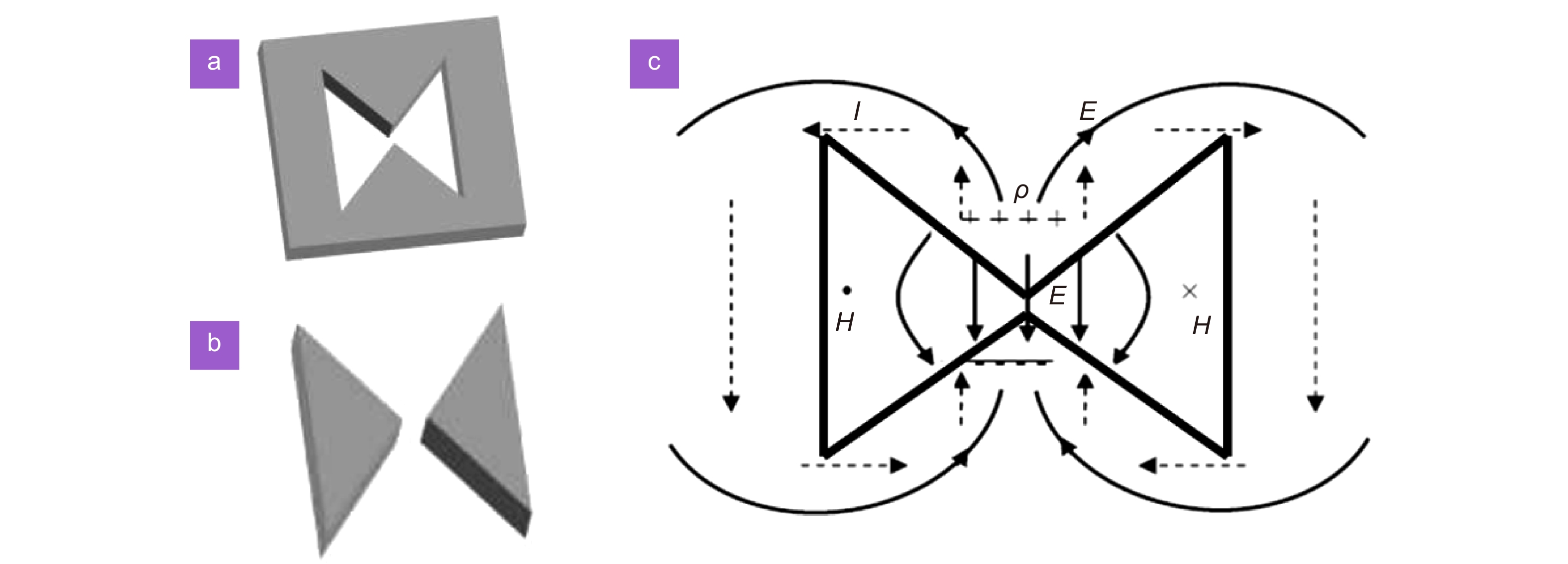
Figure 1.
Bowtie apertured (a) and gaped (b) antennas. (c) Induced surface charges and electric dipole when incident electric field polarizes along the tips. Figure reproduced with permission from: (a-b) ref.4, Copyright 2006 American Chemical Society.
-
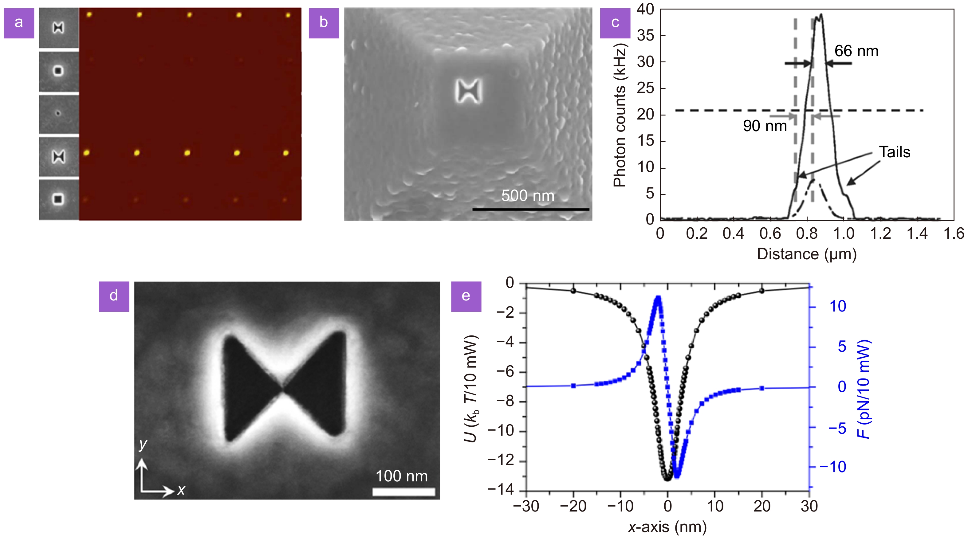
Figure 2.
Near-field imaging and trapping using (apertured) bowties. (a) Transmission through the subwavelength apertures. Bowtie apertures show much enhanced transmission. Left: different apertures. Right: far-field transmission measurements. (b) Bowtie apertures fabricated on the SNOM probe. (c) Line profiles of SNOM images using bowtie (solid line) and square (dashed line) aperture probes. (d) 5-nm-gap bowtie apertures. (e) Optical potentials U and the corresponding optical forces F along the x-axis. Figure reproduced with permission from: (a–c) ref.3, Copyright 2007 AIP Publishing; (d–e) ref.27, Copyright 2018 the author(s), under a Creative Commons Attribution 4.0 International License.
-
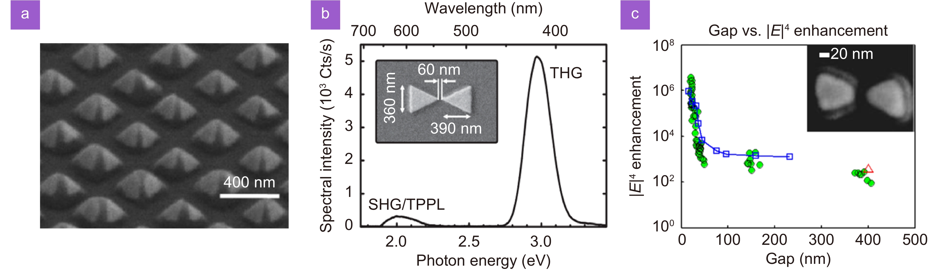
Figure 3.
Nonlinear response in bowties. (a) Three-dimensional (3D) gold bowties array. (b) Nonlinear emission spectrum from a single bowtie (inset). (c) Spectrum of generated high harmonics from 2D bowties array (inset). (d) Experimental (TPPL, circles) and theoretical (field enhancement, squares) results versus bowtie gap size. Inset shows a bowtie with a 22 nm gap. Figure reproduced with permission from: (a) ref.32, American Chemical Society; (b) ref.35, under a Creative Commons Attribution 3.0 License; (c) ref.15, American Physical Society.
-
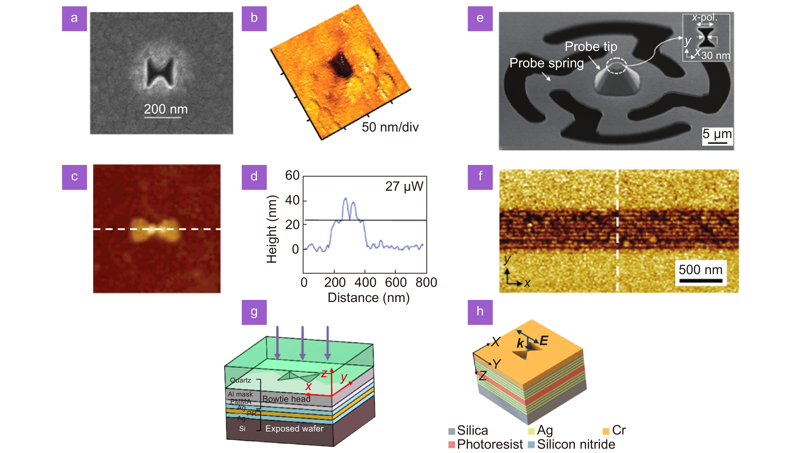
Figure 4.
Nanolithography using bowties. (a) Bowtie apertures with a 30 nm gap. (b) AFM image of 40 nm × 50 nm lithography hole. (c–d) AFM image (c) and cross section (d) along the nanoantenna axis of bowties exposed at 25 μW laser power. Feature size of ~30 nm for each of the resist pillars was measured. (e) SEM image of the fabricated circular contact probe. (f) AFM image of a 22-nm half pitch resolution line array pattern. (g–h) Bowtie nanolithography combined with metal-insulator-metal (g) and hyperbolic metamaterials (h). Figure reproduced with permission from: (a, b) ref.4, Copyright 2016 American Chemical Society; (c, d) ref.16, American Chemical Society; (e, f) ref.37, Copyright 2012 John Wiley and Sons; (g) ref.38, Copyright 2019 Optical Society of America; (h) ref.41, IOP Publishing.
-
Figure 5.
Bowtie based nanosources. (a) Schematic of 3D bowtie plasmonic lasers. (b) Evolution of lasing spectra from 3D Au bowties under pump polarization parallel to the tip axis. Inset shows emission intensity versus pump pulse energy density plotted on a semilogarithmic scale. (c) Directional SP out-coupling emission. (d) Bowties with a small gap. (e) Simulated near-field patterns of one of resonant modes in bowties. (f) Thermal emission spectrum under different bowtie gap sizes. Figure reproduced with permission from: (a–c) ref.17, Copyright 2012 American Chemical Society; (d–f) ref.44, Copyright 2017 the author(s), under the
ACS AuthorChoice via CC-BY-NC-ND Usage Agreement . -
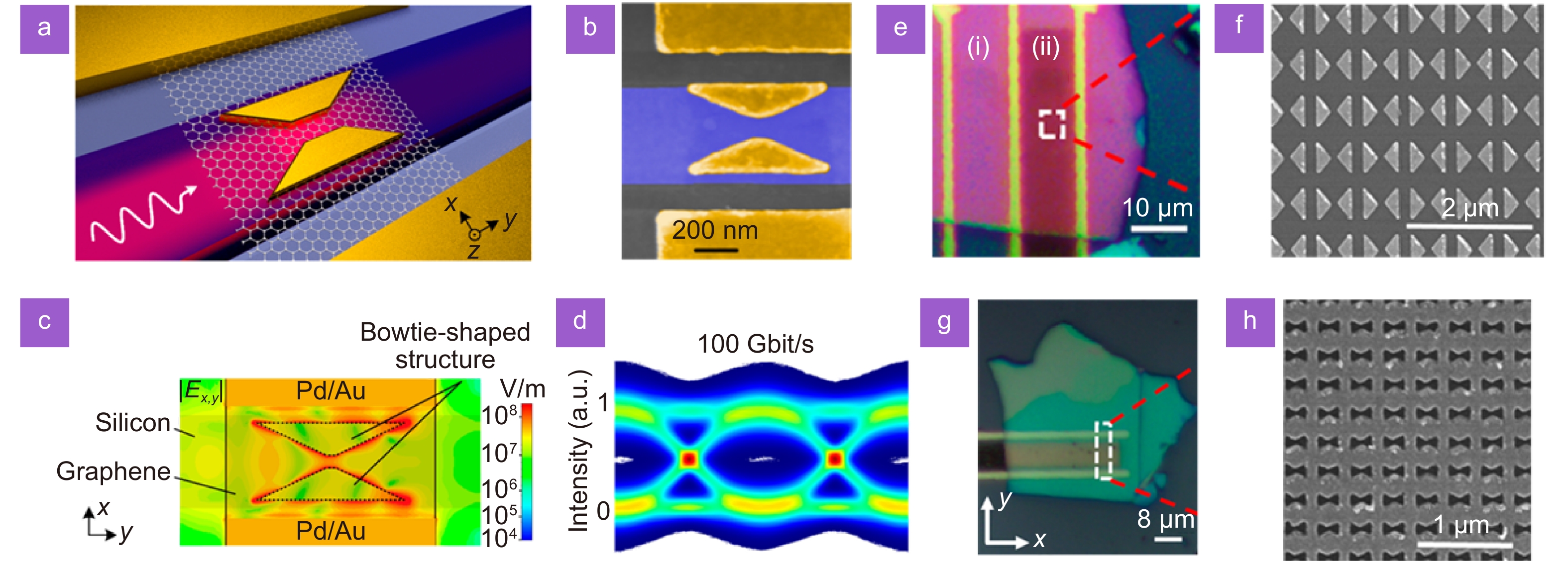
Figure 6.
2D materials photodetectors based on bowties. (a) Schematic and (b) SEM image of the plasmonically enhanced graphene photodetector. (c) The magnitude of in-plane electric fields. Strong plasmonic field enhancements in the gap were observed. (d) Eye diagram of 100 Gbit/s OOK optical signals. (e) Optical and (f) SEM image of bowtie gap antennas for high responsivity detectors. (g) Optical and (h) SEM image of bowtie aperture antennas for high polarization. Figure reproduced with permission from: (a–d) ref.45, Copyright 2019 The Author(s), under the
ACS AuthorChoice Usage Agreement ; (e–h) ref.18, Copyright 2018 American Chemical Society. -
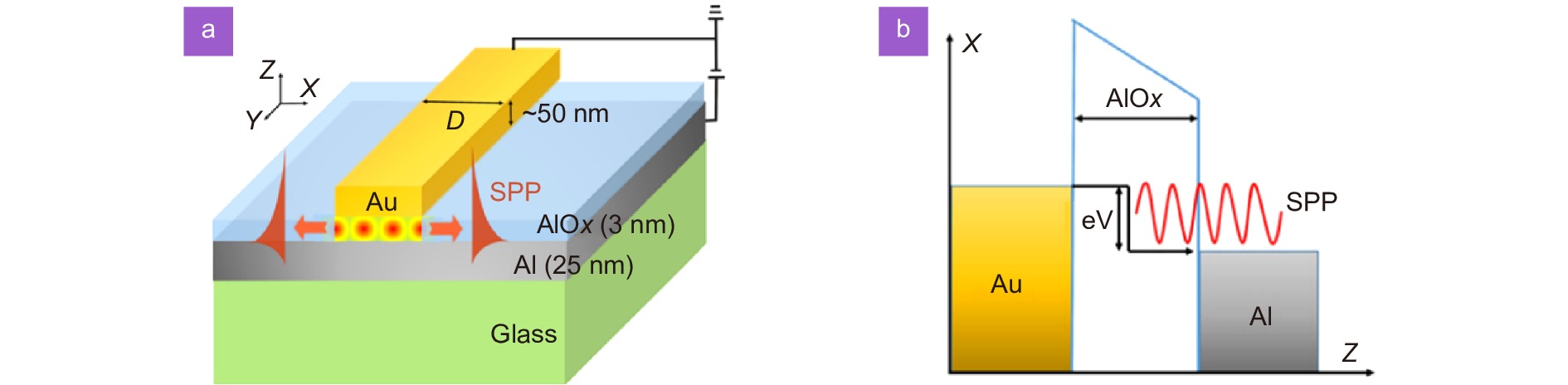
Figure 7.
Surface plasmons mediated via the IET process. (a) Schematic of the Al-AlOx-Au tunnel junction. (b) Energy level diagram of the IET process. (c) Bias dependent emission spectra. Emitted photons with cut-off frequencies can be seen. Figure reproduced with permission from ref.49, under a Creative Commons Attribution 4.0 International License.
-
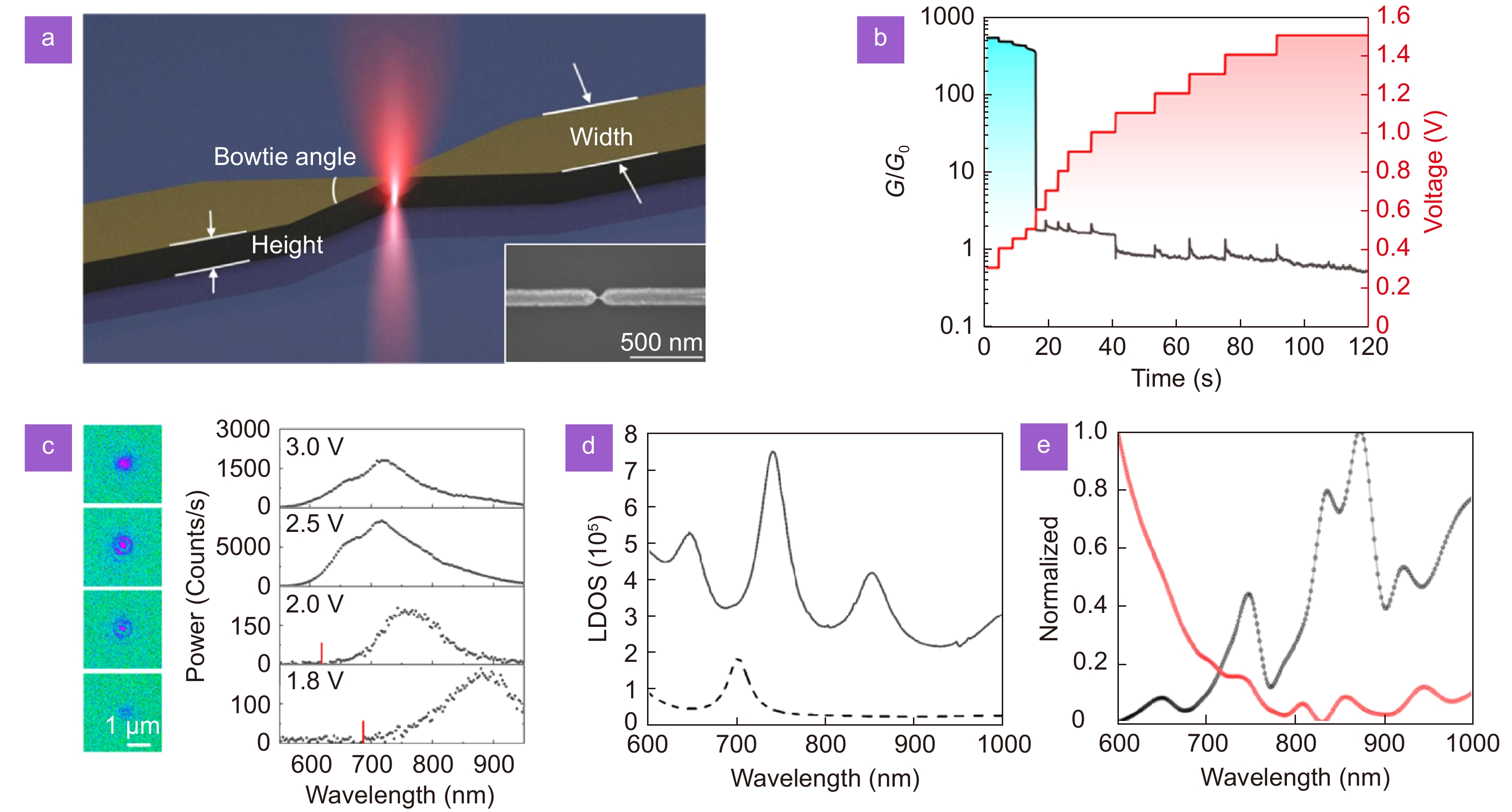
Figure 8.
Light emission from bowtie antenna based tunnel junctions. (a) Lateral tunnel junctions made by bowtie gap-antennas. Inset shows that the bowtie antennas are connected before the electro-migration process. (b) Time evolution of normalized conductance (G/G0). (c) Light emission spectra. Left column: images captured under different biases. Right column: spectral evolution under different bias. (d) Enhanced LDOS in the order of 105. Solid line: bowties case. Dashed lines: nanowire case. (e) Wavelength dependent normalized LDOS (red) and radiation efficiency (black). They both contribute to the ultimate emission spectrum. Figure reproduced with permission from: (a–d) ref.19, Copyright 2019 American Chemical Society; (e) ref.64, Copyright 2020 Optical Society of America.


