
 E-mail Alert
 RSS
RSS
| Citation: |
Elbanna A, Chaykun K, Lekina Y, Liu YD, Febriansyah B et al. Perovskite-transition metal dichalcogenides heterostructures: recent advances and future perspectives. Opto-Electron Sci 1, 220006 (2022). doi: 10.29026/oes.2022.220006

|
Perovskite-transition metal dichalcogenides heterostructures: recent advances and future perspectives
-
Abstract
Transition metal dichalcogenides (TMDs) and perovskites are among the most attractive and widely investigated semiconductors in the recent decade. They are promising materials for various applications, such as photodetection, solar energy harvesting, light emission, and many others. Combining these materials to form heterostructures can enrich the already fascinating properties and bring up new phenomena and opportunities. Work in this field is growing rapidly in both fundamental studies and device applications. Here, we review the recent findings in the perovskite-TMD heterostructures and give our perspectives on the future development of this promising field. The fundamental properties of the perovskites, TMDs, and their heterostructures are discussed first, followed by a summary of the synthesis methods of the perovskites and TMDs and the approaches to obtain high-quality interfaces. Particular attention is paid to the TMD-perovskite heterostructures that have been applied in solar cells and photodetectors with notable performance improvement. Finally through our analysis, we propose an outline on further fundamental studies and the promising applications of perovskite-TMD heterostructures.-
Keywords:
- transition metal dichalcogenides /
- perovskites /
- heterostructures /
- photodetectors /
- solar cells /
- 2D materials
-

-
References
[1] Green MA, Dunlop ED, Hohl-Ebinger J, Yoshita M, Kopidakis N et al. Solar cell efficiency tables (version 56). Prog Photovoltaics Res Appl 28, 629–638 (2020). doi: 10.1002/pip.3303 [2] Niemann RG, Kontos AG, Palles D, Kamitsos EI, Kaltzoglou A et al. Halogen effects on ordering and bonding of CH3NH3+ in CH3NH3PbX3 (X = Cl, Br, I) hybrid perovskites: a vibrational spectroscopic study. J Phys Chem C 120, 2509–2519 (2016). doi: 10.1021/acs.jpcc.5b11256 [3] Jung EH, Jeon NJ, Park EY, Moon CS, Shin TJ et al. Efficient, stable and scalable perovskite solar cells using poly(3-hexylthiophene). Nature 567, 511–515 (2019). doi: 10.1038/s41586-019-1036-3 [4] Saliba M, Matsui T, Domanski K, Seo JY, Ummadisingu A et al. Incorporation of rubidium cations into perovskite solar cells improves photovoltaic performance. Science 354, 206–209 (2016). doi: 10.1126/science.aah5557 [5] Jiang Q, Zhao Y, Zhang XW, Yang XL, Chen Y et al. Surface passivation of perovskite film for efficient solar cells. Nat Photonics 13, 460–466 (2019). doi: 10.1038/s41566-019-0398-2 [6] Chen Q, De Marco N, Yang Y, Song TB, Chen CC et al. Under the spotlight: the organic–inorganic hybrid halide perovskite for optoelectronic applications. Nano Today 10, 355–396 (2015). doi: 10.1016/j.nantod.2015.04.009 [7] Serpetzoglou E, Konidakis I, Kourmoulakis G, Demeridou I, Chatzimanolis K et al. Charge carrier dynamics in different crystal phases of CH3NH3PbI3 perovskite. Opto-Electron Sci 1, 210005 (2022). doi: 10.29026/oes.2022.210005 [8] Marshall KP, Walker M, Walton RI, Hatton RA. Enhanced stability and efficiency in hole-transport-layer-free CsSnI3 perovskite photovoltaics. Nat Energy 1, 16178 (2016). doi: 10.1038/nenergy.2016.178 [9] Saparov B, Mitzi DB. Organic–inorganic perovskites: structural versatility for functional materials design. Chem Rev 116, 4558–4596 (2016). doi: 10.1021/acs.chemrev.5b00715 [10] Zhao YX, Zhu K. Organic–inorganic hybrid lead halide perovskites for optoelectronic and electronic applications. Chem Soc Rev 45, 655–689 (2016). doi: 10.1039/C4CS00458B [11] Tsai H, Asadpour R, Blancon JC, Stoumpos CC, Durand O et al. Light-induced lattice expansion leads to high-efficiency perovskite solar cells. Science 360, 67–70 (2018). doi: 10.1126/science.aap8671 [12] Yang S, Chen SS, Mosconi E, Fang YJ, Xiao X et al. Stabilizing halide perovskite surfaces for solar cell operation with wide-bandgap lead oxysalts. Science 365, 473–478 (2019). doi: 10.1126/science.aax3294 [13] Tress W, Domanski K, Carlsen B, Agarwalla A, Alharbi EA et al. Performance of perovskite solar cells under simulated temperature-illumination real-world operating conditions. Nat Energy 4, 568–574 (2019). doi: 10.1038/s41560-019-0400-8 [14] Birowosuto MD, Cortecchia D, Drozdowski W, Brylew K, Lachmanski W et al. X-ray scintillation in lead halide perovskite crystals. Sci Rep 6, 37254 (2016). doi: 10.1038/srep37254 [15] Yakunin S, Sytnyk M, Kriegner D, Shrestha S, Richter M et al. Detection of X-ray photons by solution-processed lead halide perovskites. Nat Photonics 9, 444–449 (2015). doi: 10.1038/nphoton.2015.82 [16] Yang ZQ, Deng YH, Zhang XW, Wang S, Chen HZ et al. High-performance single-crystalline perovskite thin-film photodetector. Adv Mater 30, 1704333 (2018). doi: 10.1002/adma.201704333 [17] Li XM, Yu DJ, Chen J, Wang Y, Cao F et al. Constructing fast carrier tracks into flexible perovskite photodetectors to greatly improve responsivity. ACS Nano 11, 2015–2023 (2017). doi: 10.1021/acsnano.6b08194 [18] Hu X, Zhang XD, Liang L, Bao J, Li S et al. High-performance flexible broadband photodetector based on organolead halide perovskite. Adv Funct Mater 24, 7373–7380 (2014). doi: 10.1002/adfm.201402020 [19] Lan CY, Dong RT, Zhou ZY, Shu L, Li DP et al. Large-scale synthesis of freestanding layer-structured PbI2 and MAPbI3 nanosheets for high-performance photodetection. Adv Mater 29, 1702759 (2017). doi: 10.1002/adma.201702759 [20] Wangyang PH, Gong CH, Rao GF, Hu K, Wang XP et al. Recent advances in halide perovskite photodetectors based on different dimensional materials. Adv Opt Mater 6, 1701302 (2018). doi: 10.1002/adom.201701302 [21] Ji L, Hsu HY, Lee JC, Bard AJ, Yu ET. High-performance photodetectors based on solution-processed epitaxial grown hybrid halide perovskites. Nano Lett 18, 994–1000 (2018). doi: 10.1021/acs.nanolett.7b04445 [22] Tan ZJ, Wu Y, Hong H, Yin JB, Zhang JC et al. Two-dimensional (C4H9NH3)2PbBr4 perovskite crystals for high-performance photodetector. J Am Chem Soc 138, 16612–16615 (2016). doi: 10.1021/jacs.6b11683 [23] Lin YH, Pattanasattayavong P, Anthopoulos TD. Metal‐halide perovskite transistors for printed electronics: challenges and opportunities. Adv Mater 29, 1702838 (2017). doi: 10.1002/adma.201702838 [24] Pan WC, Wu HD, Luo JJ, Deng ZZ, Ge C et al. Cs2AgBiBr6 single-crystal X-ray detectors with a low detection limit. Nat Photonics 11, 726–732 (2017). doi: 10.1038/s41566-017-0012-4 [25] Wei HT, Huang JS. Halide lead perovskites for ionizing radiation detection. Nat Commun 10, 1066 (2019). doi: 10.1038/s41467-019-08981-w [26] Pedesseau L, Sapori D, Traore B, Robles R, Fang HH et al. Advances and promises of layered halide hybrid perovskite semiconductors. ACS Nano 10, 9776–9786 (2016). doi: 10.1021/acsnano.6b05944 [27] Ramirez D, Suto Y, Rosero-Navarro NC, Miura A, Tadanaga K et al. Structural and electrochemical evaluation of three- and two-dimensional organohalide perovskites and their influence on the reversibility of lithium intercalation. Inorg Chem 57, 4181–4188 (2018). doi: 10.1021/acs.inorgchem.8b00397 [28] Smith MD, Connor BA, Karunadasa HI. Tuning the luminescence of layered halide perovskites. Chem Rev 119, 3104–3139 (2019). doi: 10.1021/acs.chemrev.8b00477 [29] Li ZT, Cao K, Li JS, Tang Y, Ding XR et al. Review of blue perovskite light emitting diodes with optimization strategies for perovskite film and device structure. Opto-Electron Adv 4, 200019 (2021). doi: 10.29026/oea.2021.200019 [30] Lai ML, Tay TYS, Sadhanala A, Dutton SE, Li GR et al. Tunable near-infrared luminescence in Tin halide perovskite devices. J Phys Chem Lett 7, 2653–2658 (2016). doi: 10.1021/acs.jpclett.6b01047 [31] Wong AB, Lai ML, Eaton SW, Yu Y, Lin E et al. Growth and anion exchange conversion of CH3NH3PbX3 nanorod arrays for light-emitting diodes. Nano Lett 15, 5519–5524 (2015). doi: 10.1021/acs.nanolett.5b02082 [32] Leyden MR, Meng LQ, Jiang Y, Ono LK, Qiu LB et al. Methylammonium lead bromide perovskite light-emitting diodes by chemical vapor deposition. J Phys Chem Lett 8, 3193–3198 (2017). doi: 10.1021/acs.jpclett.7b01093 [33] Yuan S, Wang ZK, Zhuo MP, Tian QS, Jin Y et al. Self-assembled high quality CsPbBr3 quantum dot films toward highly efficient light-emitting diodes. ACS Nano 12, 9541–9548 (2018). doi: 10.1021/acsnano.8b05185 [34] Cho H, Kim YH, Wolf C, Lee HD, Lee TW. Improving the stability of metal halide perovskite materials and light-emitting diodes. Adv Mater 30, 1704587 (2018). doi: 10.1002/adma.201704587 [35] Raghavan CM, Chen TP, Li SS, Chen WL, Lo CY et al. Low-threshold lasing from 2D homologous organic–inorganic hybrid ruddlesden–popper perovskite single crystals. Nano Lett 18, 3221–3228 (2018). doi: 10.1021/acs.nanolett.8b00990 [36] Wei Q, Li XJ, Liang C, Zhang ZP, Guo J et al. Recent progress in metal halide perovskite micro‐ and nanolasers. Adv Opt Mater 7, 1900080 (2019). doi: 10.1002/adom.201900080 [37] Wang KY, Xing GC, Song QH, Xiao SM. Micro‐ and nanostructured lead halide perovskites: from materials to integrations and devices. Adv Mater 33, 2000306 (2021). doi: 10.1002/adma.202000306 [38] Qin CJ, Sandanayaka ASD, Zhao CY, Matsushima T, Zhang DZ et al. Stable room-temperature continuous-wave lasing in quasi-2D perovskite films. Nature 585, 53–57 (2020). doi: 10.1038/s41586-020-2621-1 [39] Xing GC, Mathews N, Lim SS, Yantara N, Liu XF et al. Low-temperature solution-processed wavelength-tunable perovskites for lasing. Nat Mater 13, 476–480 (2014). doi: 10.1038/nmat3911 [40] El-Ballouli AO, Bakr OM, Mohammed OF. Structurally tunable two-dimensional layered perovskites: from confinement and enhanced charge transport to prolonged hot carrier cooling dynamics. J Phys Chem Lett 11, 5705–5718 (2020). doi: 10.1021/acs.jpclett.0c00359 [41] Quan LN, Yuan MJ, Comin R, Voznyy O, Beauregard EM et al. Ligand-stabilized reduced-dimensionality perovskites. J Am Chem Soc 138, 2649–2655 (2016). doi: 10.1021/jacs.5b11740 [42] Jung MH. Photovoltaic effect of 2D homologous perovskites. Electrochim Acta 240, 98–107 (2017). doi: 10.1016/j.electacta.2017.04.067 [43] Tsai H, Nie WY, Blancon JC, Stoumpos CC, Asadpour R et al. High-efficiency two-dimensional ruddlesden–popper perovskite solar cells. Nature 536, 312–316 (2016). doi: 10.1038/nature18306 [44] Blancon JC, Tsai H, Nie W, Stoumpos CC, Pedesseau L et al. Extremely efficient internal exciton dissociation through edge states in layered 2D perovskites. Science 355, 1288–1292 (2017). doi: 10.1126/science.aal4211 [45] Stoumpos CC, Soe CMM, Tsai H, Nie WY, Blancon JC et al. High members of the 2D ruddlesden-popper halide perovskites: synthesis, optical properties, and solar cells of (CH3(CH2)3NH3)2(CH3NH3)4Pb5I16. Chem 2, 427–440 (2017). doi: 10.1016/j.chempr.2017.02.004 [46] Gan XY, Wang O, Liu KY, Du XJ, Guo LL et al. 2D homologous organic-inorganic hybrids as light-absorbers for planer and nanorod-based perovskite solar cells. Sol Energy Mater Sol Cells 162, 93–102 (2017). doi: 10.1016/j.solmat.2016.12.047 [47] Wei Y, Audebert P, Galmiche L, Lauret JS, Deleporte E. Photostability of 2D organic-inorganic hybrid perovskites. Materials 7, 4789–4802 (2014). doi: 10.3390/ma7064789 [48] Wang NN, Cheng L, Ge R, Zhang ST, Miao YF et al. Perovskite light-emitting diodes based on solution-processed self-organized multiple quantum wells. Nat Photonics 10, 699–704 (2016). doi: 10.1038/nphoton.2016.185 [49] Yuan MJ, Quan LN, Comin R, Walters G, Sabatini R et al. Perovskite energy funnels for efficient light-emitting diodes. Nat Nanotechnol 11, 872–877 (2016). doi: 10.1038/nnano.2016.110 [50] Li D, Liao PZ, Shai XX, Huang WC, Liu SS et al. Recent progress on stability issues of organic–inorganic hybrid lead perovskite-based solar cells. RSC Adv 6, 89356–89366 (2016). doi: 10.1039/C6RA19801E [51] Wang ZP, Lin QQ, Chmiel FP, Sakai N, Herz LM et al. Efficient ambient-air-stable solar cells with 2D–3D heterostructured butylammonium-caesium-formamidinium lead halide perovskites. Nat Energy 2, 17135 (2017). doi: 10.1038/nenergy.2017.135 [52] Long MS, Wang P, Fang HH, Hu WD. Progress, challenges, and opportunities for 2D material based photodetectors. Adv Funct Mater 29, 1803807 (2019). doi: 10.1002/adfm.201803807 [53] Huo NJ, Konstantatos G. Recent progress and future prospects of 2D-based photodetectors. Adv Mater 30, 1801164 (2018). doi: 10.1002/adma.201801164 [54] Wang FK, Zhang Y, Gao Y, Luo P, Su JW et al. 2D metal chalcogenides for IR photodetection. Small 15, 1901347 (2019). doi: 10.1002/smll.201901347 [55] Xie C, Mak C, Tao XM, Yan F. Photodetectors based on two-dimensional layered materials beyond graphene. Adv Funct Mater 27, 1603886 (2017). doi: 10.1002/adfm.201603886 [56] Mitta SB, Choi MS, Nipane A, Ali F, Kim C et al. Electrical characterization of 2D materials-based field-effect transistors. 2D Mater 8, 012002 (2021). doi: 10.1088/2053-1583/abc187 [57] Shang JZ, Cong CX, Wu LS, Huang W, Yu T. Light sources and photodetectors enabled by 2D semiconductors. Small Methods 2, 1800019 (2018). doi: 10.1002/smtd.201800019 [58] Lien DH, Amani M, Desai SB, Ahn GH, Han K et al. Large-area and bright pulsed electroluminescence in monolayer semiconductors. Nat Commun 9, 1229 (2018). doi: 10.1038/s41467-018-03218-8 [59] Ross JS, Klement P, Jones AM, Ghimire NJ, Yan JQ et al. Electrically tunable excitonic light-emitting diodes based on monolayer WSe2 p–n junctions. Nat Nanotechnol 9, 268–272 (2014). doi: 10.1038/nnano.2014.26 [60] Withers F, Del Pozo-Zamudio O, Mishchenko A, Rooney AP, Gholinia A et al. Light-emitting diodes by band-structure engineering in van der Waals heterostructures. Nat Mater 14, 301–306 (2015). doi: 10.1038/nmat4205 [61] Mak KF, Shan J. Photonics and optoelectronics of 2D semiconductor transition metal dichalcogenides. Nat Photonics 10, 216–226 (2016). doi: 10.1038/nphoton.2015.282 [62] Wu SF, Buckley S, Schaibley JR, Feng LF, Yan JQ et al. Monolayer semiconductor nanocavity lasers with ultralow thresholds. Nature 520, 69–72 (2015). doi: 10.1038/nature14290 [63] Ye Y, Wong ZJ, Lu XF, Ni XJ, Zhu HY et al. Monolayer excitonic laser. Nat Photonics 9, 733–737 (2015). doi: 10.1038/nphoton.2015.197 [64] Liu ML, Wu HB, Liu XM, Wang YR, Lei M et al. Optical properties and applications of SnS2 SAs with different thickness. Opto-Electron Adv 4, 200029 (2021). doi: 10.29026/oea.2021.200029 [65] Li YZ, Zhang JX, Huang DD, Sun H, Fan F et al. Room-temperature continuous-wave lasing from monolayer molybdenum ditelluride integrated with a silicon nanobeam cavity. Nat Nanotechnol 12, 987–992 (2017). doi: 10.1038/nnano.2017.128 [66] Liu YD, Fang HL, Rasmita A, Zhou Y, Li JT et al. Room temperature nanocavity laser with interlayer excitons in 2D heterostructures. Sci Adv 5, eaav4506 (2019). doi: 10.1126/sciadv.aav4506 [67] Shang JZ, Cong CX, Wang ZL, Peimyoo N, Wu LS et al. Room-temperature 2D semiconductor activated vertical-cavity surface-emitting lasers. Nat Commun 8, 543 (2017). doi: 10.1038/s41467-017-00743-w [68] Bernardi M, Palummo M, Grossman JC. Extraordinary sunlight absorption and one nanometer thick photovoltaics using two-dimensional monolayer materials. Nano Lett 13, 3664–3670 (2013). doi: 10.1021/nl401544y [69] Sumesh CK. Towards efficient photon management in nanostructured solar cells: role of 2D layered transition metal dichalcogenide semiconductors. Sol Energy Mater Sol Cells 192, 16–23 (2019). doi: 10.1016/j.solmat.2018.12.016 [70] Lin YB, Adilbekova B, Firdaus Y, Yengel E, Faber H et al. 17% efficient organic solar cells based on liquid exfoliated WS2 as a replacement for PEDOT: PSS. Adv Mater 31, 1902965 (2019). doi: 10.1002/adma.201902965 [71] Rivera P, Yu HY, Seyler KL, Wilson NP, Yao W et al. Interlayer valley excitons in heterobilayers of transition metal dichalcogenides. Nat Nanotechnol 13, 1004–1015 (2018). doi: 10.1038/s41565-018-0193-0 [72] Flöry N, Ma P, Salamin Y, Emboras A, Taniguchi T et al. Waveguide-integrated van der Waals heterostructure photodetector at telecom wavelengths with high speed and high responsivity. Nat Nanotechnol 15, 118–124 (2020). doi: 10.1038/s41565-019-0602-z [73] Zhang L, Wu FC, Hou SC, Zhang Z, Chou YH et al. Van der Waals heterostructure polaritons with moiré-induced nonlinearity. Nature 591, 61–65 (2021). doi: 10.1038/s41586-021-03228-5 [74] Jiang CY, Xu WG, Rasmita A, Huang ZM, Li K et al. Microsecond dark-exciton valley polarization memory in two-dimensional heterostructures. Nat Commun 9, 753 (2018). doi: 10.1038/s41467-018-03174-3 [75] Shimazaki Y, Schwartz I, Watanabe K, Taniguchi T, Kroner M et al. Strongly correlated electrons and hybrid excitons in a moiré heterostructure. Nature 580, 472–477 (2020). doi: 10.1038/s41586-020-2191-2 [76] Tran K, Moody G, Wu FC, Lu XB, Choi J et al. Evidence for moiré excitons in van der Waals heterostructures. Nature 567, 71–75 (2019). doi: 10.1038/s41586-019-0975-z [77] Jin CH, Regan EC, Yan AM, Utama MIB, Wang DQ et al. Observation of moiré excitons in WSe2/WS2 heterostructure superlattices. Nature 567, 76–80 (2019). doi: 10.1038/s41586-019-0976-y [78] Brotons-Gisbert M, Baek H, Molina-Sánchez A, Campbell A, Scerri E et al. Spin–layer locking of interlayer excitons trapped in moiré potentials. Nat Mater 19, 630–636 (2020). doi: 10.1038/s41563-020-0687-7 [79] Alexeev EM, Ruiz-Tijerina DA, Danovich M, Hamer MJ, Terry DJ et al. Resonantly hybridized excitons in moiré superlattices in van der Waals heterostructures. Nature 567, 81–86 (2019). doi: 10.1038/s41586-019-0986-9 [80] Li WJ, Lu X, Dubey S, Devenica L, Srivastava A. Dipolar interactions between localized interlayer excitons in van der Waals heterostructures. Nat Mater 19, 624–629 (2020). doi: 10.1038/s41563-020-0661-4 [81] Chhowalla M, Shin HS, Eda G, Li LJ, Loh KP et al. The chemistry of two-dimensional layered transition metal dichalcogenide nanosheets. Nat Chem 5, 263–275 (2013). doi: 10.1038/nchem.1589 [82] Eda G, Maier SA. Two-dimensional crystals: managing light for optoelectronics. ACS Nano 7, 5660–5665 (2013). doi: 10.1021/nn403159y [83] Singh R, Singh P, Balasubramanian G. Effect of heterostructure engineering on electronic structure and transport properties of two-dimensional halide perovskites. Comput Mater Sci 200, 110823 (2021). doi: 10.1016/j.commatsci.2021.110823 [84] Ricciardulli AG, Yang S, Smet JH, Saliba M. Emerging perovskite monolayers. Nat Mater 20, 1325–1336 (2021). doi: 10.1038/s41563-021-01029-9 [85] Chen YY, Liu ZY, Li JZ, Cheng X, Ma JQ et al. Robust interlayer coupling in two-dimensional perovskite/monolayer transition metal dichalcogenide heterostructures. ACS Nano 14, 10258–10264 (2020). doi: 10.1021/acsnano.0c03624 [86] Nayak PK, Horbatenko Y, Ahn S, Kim G, Lee JU et al. Probing evolution of twist-angle-dependent interlayer excitons in MoSe2/WSe2 van der Waals Heterostructures. ACS Nano 11, 4041–4050 (2017). doi: 10.1021/acsnano.7b00640 [87] Lo SS, Mirkovic T, Chuang CH, Burda C, Scholes GD. Emergent properties resulting from type-II band alignment in semiconductor nanoheterostructures. Adv Mater 23, 180–197 (2011). doi: 10.1002/adma.201002290 [88] Liu HY, Tan YS, Cao MH, Hu HC, Wu LZ et al. Fabricating CsPbX3-based type I and type II heterostructures by tuning the halide composition of janus CsPbX3/ZrO2 nanocrystals. ACS Nano 13, 5366–5374 (2019). doi: 10.1021/acsnano.9b00001 [89] Fang QY, Shang QY, Zhao LY, Wang R, Zhang ZP et al. Ultrafast charge transfer in perovskite nanowire/2D transition metal dichalcogenide heterostructures. J Phys Chem Lett 9, 1655–1662 (2018). doi: 10.1021/acs.jpclett.8b00260 [90] Wang Y, Fullon R, Acerce M, Petoukhoff CE, Yang J et al. Solution-processed MoS2/organolead trihalide perovskite photodetectors. Adv Mater 29, 1603995 (2017). doi: 10.1002/adma.201603995 [91] Wang LM, Zou XM, Lin J, Jiang JY, Liu Y et al. Perovskite/black phosphorus/MoS2 photogate reversed photodiodes with ultrahigh light on/off ratio and fast response. ACS Nano 13, 4804–4813 (2019). doi: 10.1021/acsnano.9b01713 [92] Wu HL, Kang Z, Zhang ZH, Zhang Z, Si HN et al. Interfacial charge behavior modulation in perovskite quantum dot-monolayer MoS2 0D-2D mixed-dimensional van der waals heterostructures. Adv Funct Mater 28, 1802015 (2018). doi: 10.1002/adfm.201802015 [93] Yang A, Blancon JC, Jiang W, Zhang H, Wong J et al. Giant enhancement of photoluminescence emission in WS2-two-dimensional perovskite heterostructures. Nano Lett 19, 4852–4860 (2019). doi: 10.1021/acs.nanolett.8b05105 [94] Wang XD, Huang YH, Liao JF, Jiang Y, Zhou L et al. In situ construction of a Cs2SnI6 perovskite nanocrystal/SnS2 nanosheet heterojunction with boosted interfacial charge transfer. J Am Chem Soc 141, 13434–13441 (2019). doi: 10.1021/jacs.9b04482 [95] Zhang Q, Linardy E, Wang XY, Eda G. Excitonic energy transfer in heterostructures of quasi-2D perovskite and monolayer WS2. ACS Nano 14, 11482–11489 (2020). doi: 10.1021/acsnano.0c03893 [96] Wang HZ, Ma JQ, Li DH. Two-dimensional hybrid perovskite-based van der waals heterostructures. J Phys Chem Lett 12, 8178–8187 (2021). doi: 10.1021/acs.jpclett.1c02290 [97] Shi EZ, Gao Y, Finkenauer BP, Akriti, Coffey AH et al. Two-dimensional halide perovskite nanomaterials and heterostructures. Chem Soc Rev 47, 6046–6072 (2018). doi: 10.1039/C7CS00886D [98] Xie C, Liu CK, Loi HL, Yan F. Perovskite‐based phototransistors and hybrid photodetectors. Adv Funct Mater 30, 1903907 (2020). doi: 10.1002/adfm.201903907 [99] Omprakash P, Viswesh P, Devadas BP. Review—a review of 2D perovskites and carbon-based nanomaterials for applications in solar cells and photodetectors. ECS J Solid State Sci Technol 10, 031009 (2021). doi: 10.1149/2162-8777/abefaf [100] Ghosh J, Giri PK. Recent advances in perovskite/2D materials based hybrid photodetectors. J Phys Mater 4, 032008 (2021). doi: 10.1088/2515-7639/abf544 [101] Bellani S, Bartolotta A, Agresti A, Calogero G, Grancini G et al. Solution-processed two-dimensional materials for next-generation photovoltaics. Chem Soc Rev 50, 11870–11965 (2021). doi: 10.1039/D1CS00106J [102] Rogdakis K, Karakostas N, Kymakis E. Up-scalable emerging energy conversion technologies enabled by 2D materials: from miniature power harvesters towards grid-connected energy systems. Energy Environ Sci 14, 3352–3392 (2021). doi: 10.1039/D0EE04013D [103] Pant A, Mutlu Z, Wickramaratne D, Cai H, Lake RK et al. Fundamentals of lateral and vertical heterojunctions of atomically thin materials. Nanoscale 8, 3870–3887 (2016). doi: 10.1039/C5NR08982D [104] Unger EL, Kegelmann L, Suchan K, Sörell D, Korte L et al. Roadmap and roadblocks for the band gap tunability of metal halide perovskites. J Mater Chem A 5, 11401–11409 (2017). doi: 10.1039/C7TA00404D [105] Jiang Y, Chen SL, Zheng WH, Zheng BY, Pan AL. Interlayer exciton formation, relaxation, and transport in TMD van der Waals heterostructures. Light Sci Appl 10, 72 (2021). doi: 10.1038/s41377-021-00500-1 [106] Tartakovskii A. Excitons in 2D heterostructures. Nat Rev Phys 2, 8–9 (2020). doi: 10.1038/s42254-019-0136-1 [107] Mueller T, Malic E. Exciton physics and device application of two-dimensional transition metal dichalcogenide semiconductors. npj 2D Mater Appl 2, 29 (2018). doi: 10.1038/s41699-018-0074-2 [108] Rasmussen FA, Thygesen KS. Computational 2D materials database: electronic structure of transition-metal dichalcogenides and oxides. J Phys Chem C 119, 13169–13183 (2015). doi: 10.1021/acs.jpcc.5b02950 [109] Chaves A, Azadani JG, Alsalman H, Da Costa DR, Frisenda R et al. Bandgap engineering of two-dimensional semiconductor materials. npj 2D Mater Appl 4, 29 (2020). doi: 10.1038/s41699-020-00162-4 [110] Hong XP, Kim J, Shi SF, Zhang Y, Jin CH et al. Ultrafast charge transfer in atomically thin MoS2/WS2 heterostructures. Nat Nanotechnol 9, 682–686 (2014). doi: 10.1038/nnano.2014.167 [111] Ceballos F, Bellus MZ, Chiu HY, Zhao H. Ultrafast charge separation and indirect exciton formation in a MoS2–MoSe2 van der waals heterostructure. ACS Nano 8, 12717–12724 (2014). doi: 10.1021/nn505736z [112] Jin CH, Ma EY, Karni O, Regan EC, Wang F et al. Ultrafast dynamics in van der waals heterostructures. Nat Nanotechnol 13, 994–1003 (2018). doi: 10.1038/s41565-018-0298-5 [113] Mak KF, Shan J. Opportunities and challenges of interlayer exciton control and manipulation. Nat Nanotechnol 13, 974–976 (2018). doi: 10.1038/s41565-018-0301-1 [114] Excitation that lasts. Nat Nanotechnol 13, 973 (2018). [115] Liu Y, Weiss NO, Duan XD, Cheng HC, Huang Y et al. Van der waals heterostructures and devices. Nat Rev Mater 1, 16042 (2016). doi: 10.1038/natrevmats.2016.42 [116] Liu YD, Elbanna A, Gao WB, Pan JS, Shen ZX et al. Interlayer excitons in transition metal dichalcogenide semiconductors for 2D optoelectronics. Adv Mater 34, 2107138 (2022). doi: 10.1002/adma.202107138 [117] Lukman S, Ding L, Xu L, Tao Y, Riis-Jensen AC et al. High oscillator strength interlayer excitons in two-dimensional heterostructures for mid-infrared photodetection. Nat Nanotechnol 15, 675–682 (2020). doi: 10.1038/s41565-020-0717-2 [118] Karni O, Barré E, Lau SC, Gillen R, Ma EY et al. Infrared interlayer exciton emission in MoS2/WSe2 heterostructures. Phys Rev Lett 123, 247402 (2019). doi: 10.1103/PhysRevLett.123.247402 [119] Wang ZF, Rhodes DA, Watanabe K, Taniguchi T, Hone JC et al. Evidence of high-temperature exciton condensation in two-dimensional atomic double layers. Nature 574, 76–80 (2019). doi: 10.1038/s41586-019-1591-7 [120] Kim J, Jin CH, Cai H, Zhao T, Lee P et al. Observation of ultralong valley lifetime in WSe2/MoS2 heterostructures. Sci Adv 3, e1700518 (2017). doi: 10.1126/sciadv.1700518 [121] Jin CH, Tao Z, Li TX, Xu Y, Tang TH et al. Stripe phases in WSe2/WS2 moiré superlattices. Nat Mater 20, 940–944 (2021). doi: 10.1038/s41563-021-00959-8 [122] Regan EC, Wang DQ, Jin CH, Utama MIB, Gao BN et al. Mott and generalized wigner crystal states in WSe2/WS2 moiré superlattices. Nature 579, 359–363 (2020). doi: 10.1038/s41586-020-2092-4 [123] Abouelkomsan A, Liu Z, Bergholtz EJ. Particle-hole duality, emergent fermi liquids, and fractional chern insulators in moiré flatbands. Phys Rev Lett 124, 106803 (2020). doi: 10.1103/PhysRevLett.124.106803 [124] Xu Y, Liu S, Rhodes DA, Watanabe K, Taniguchi T et al. Correlated insulating states at fractional fillings of moiré superlattices. Nature 587, 214–218 (2020). doi: 10.1038/s41586-020-2868-6 [125] Tartakovskii A. Moiré or not. Nat Mater 19, 581–582 (2020). doi: 10.1038/s41563-020-0693-9 [126] Khelifa R, Back P, Flöry N, Nashashibi S, Malchow K et al. Coupling interlayer excitons to whispering gallery modes in van der waals heterostructures. Nano Lett 20, 6155–6161 (2020). doi: 10.1021/acs.nanolett.0c02432 [127] Paik EY, Zhang L, Burg GW, Gogna R, Tutuc E et al. Interlayer exciton laser of extended spatial coherence in atomically thin heterostructures. Nature 576, 80–84 (2019). doi: 10.1038/s41586-019-1779-x [128] Xue H, Wang YD, Dai YY, Kim W, Jussila H et al. A MoSe2/WSe2 heterojunction-based photodetector at telecommunication wavelengths. Adv Funct Mater 28, 1804388 (2018). doi: 10.1002/adfm.201804388 [129] Wang GC, Li L, Fan WH, Wang RY, Zhou SS et al. Interlayer coupling induced infrared response in WS2/MoS2 heterostructures enhanced by surface plasmon resonance. Adv Funct Mater 28, 1800339 (2018). doi: 10.1002/adfm.201800339 [130] Jo SH, Lee HW, Shim J, Heo K, Kim M et al. Highly efficient infrared photodetection in a gate-controllable van der waals heterojunction with staggered bandgap alignment. Adv Sci 5, 1700423 (2018). doi: 10.1002/advs.201700423 [131] Ross JS, Rivera P, Schaibley J, Lee-Wong E, Yu HY et al. Interlayer exciton optoelectronics in a 2D heterostructure p–n junction. Nano Lett 17, 638–643 (2017). doi: 10.1021/acs.nanolett.6b03398 [132] Zhang KN, Zhang TN, Cheng GH, Li TX, Wang SX et al. Interlayer transition and infrared photodetection in atomically thin type-II MoTe2/MoS2 van der waals heterostructures. ACS Nano 10, 3852–3858 (2016). doi: 10.1021/acsnano.6b00980 [133] Li ZD, Lu XB, Leon DFC, Lyu ZY, Xie HC et al. Interlayer exciton transport in MoSe2/WSe2 heterostructures. ACS Nano 15, 1539–1547 (2021). doi: 10.1021/acsnano.0c08981 [134] Yuan L, Zheng BY, Kunstmann J, Brumme T, Kuc AB et al. Twist-angle-dependent interlayer exciton diffusion in WS2–WSe2 heterobilayers. Nat Mater 19, 617–623 (2020). doi: 10.1038/s41563-020-0670-3 [135] Liu YD, Dini K, Tan QH, Liew T, Novoselov KS et al. Electrically controllable router of interlayer excitons. Sci Adv 6, eaba1830 (2020). doi: 10.1126/sciadv.aba1830 [136] Unuchek D, Ciarrocchi A, Avsar A, Sun Z, Watanabe K et al. Valley-polarized exciton currents in a van der Waals heterostructure. Nat Nanotechnol 14, 1104–1109 (2019). doi: 10.1038/s41565-019-0559-y [137] Jauregui LA, Joe AY, Pistunova K, Wild DS, High AA et al. Electrical control of interlayer exciton dynamics in atomically thin heterostructures. Science 366, 870–875 (2019). doi: 10.1126/science.aaw4194 [138] Ciarrocchi A, Unuchek D, Avsar A, Watanabe K, Taniguchi T et al. Polarization switching and electrical control of interlayer excitons in two-dimensional van der Waals heterostructures. Nat Photonics 13, 131–136 (2019). doi: 10.1038/s41566-018-0325-y [139] Unuchek D, Ciarrocchi A, Avsar A, Watanabe K, Taniguchi T et al. Room-temperature electrical control of exciton flux in a van der Waals heterostructure. Nature 560, 340–344 (2018). doi: 10.1038/s41586-018-0357-y [140] Jiang CY, Rasmita A, Ma H, Tan QH, Huang ZM et al. Room-temperature bipolar valleytronic transistor in MoS2/WSe2 heterostructures. arXiv:2102.03756. [141] Green MA, Dunlop ED, Hohl-Ebinger J, Yoshita M, Kopidakis N et al. Solar cell efficiency tables (Version 58). Prog Photovolt Res Appl 29, 657–667 (2021). doi: 10.1002/pip.3444 [142] Saliba M, Correa-Baena JP, Grätzel M, Hagfeldt A, Abate A. Perovskite solar cells: from the atomic level to film quality and device performance. Angew Chem Int Ed 57, 2554–2569 (2018). doi: 10.1002/anie.201703226 [143] Schileo G, Grancini G. Halide perovskites: current issues and new strategies to push material and device stability. J Phys Energy 2, 021005 (2020). doi: 10.1088/2515-7655/ab6cc4 [144] Lekina Y, Shen ZX. Excitonic states and structural stability in two-dimensional hybrid organic-inorganic perovskites. J Sci Adv Mater Dev 4, 189–200 (2019). doi: 10.1016/j.jsamd.2019.03.005 [145] Ahmad S, Fu P, Yu SW, Yang Q, Liu X et al. Dion-jacobson phase 2D layered perovskites for solar cells with ultrahigh stability. Joule 3, 794–806 (2019). doi: 10.1016/j.joule.2018.11.026 [146] Cohen BE, Wierzbowska M, Etgar L. High efficiency and high open circuit voltage in quasi 2D perovskite based solar cells. Adv Funct Mater 27, 1604733 (2017). doi: 10.1002/adfm.201604733 [147] Dou LT, Wong AB, Yu Y, Lai ML, Kornienko N et al. Atomically thin two-dimensional organic-inorganic hybrid perovskites. Science 349, 1518–1521 (2015). doi: 10.1126/science.aac7660 [148] Niu W, Eiden A, Prakash GV, Baumberg JJ. Exfoliation of self-assembled 2D organic-inorganic perovskite semiconductors. Appl Phys Lett 104, 171111 (2014). doi: 10.1063/1.4874846 [149] Dhanabalan B, Castelli A, Palei M, Spirito D, Manna L et al. Simple fabrication of layered halide perovskite platelets and enhanced photoluminescence from mechanically exfoliated flakes. Nanoscale 11, 8334–8342 (2019). doi: 10.1039/C9NR00638A [150] Fu YP, Zheng WH, Wang XX, Hautzinger MP, Pan DX. et al. Multicolor heterostructures of two-dimensional layered halide perovskites that show interlayer energy transfer. J Am Chem Soc 140, 15675–15683 (2018). doi: 10.1021/jacs.8b07843 [151] Shi EZ, Yuan B, Shiring SB, Gao Y, Akriti et al. Two-dimensional halide perovskite lateral epitaxial heterostructures. Nature 580, 614–620 (2020). doi: 10.1038/s41586-020-2219-7 [152] Akriti, Shi EZ, Shiring SB, Yang JQ, Atencio-Martinez CL et al. Layer-by-layer anionic diffusion in two-dimensional halide perovskite vertical heterostructures. Nat Nanotechnol 16, 584–591 (2021). doi: 10.1038/s41565-021-00848-w [153] Kuo MY, Spitha N, Hautzinger MP, Hsieh PL, Li J et al. Distinct carrier transport properties across horizontally vs vertically oriented heterostructures of 2D/3D perovskites. J Am Chem Soc 143, 4969–4978 (2021). doi: 10.1021/jacs.0c10000 [154] Zhang XY, Liu XT, Li LN, Ji CM, Yao YP et al. Great amplification of circular polarization sensitivity via heterostructure engineering of a chiral two-dimensional hybrid perovskite crystal with a three-dimensional MAPbI3 crystal. ACS Cent Sci 7, 1261–1268 (2021). doi: 10.1021/acscentsci.1c00649 [155] Karpińska M, Liang MP, Kempt R, Finzel K, Kamminga M et al. Nonradiative energy transfer and selective charge transfer in a WS2/(PEA)2PbI4 heterostructure. ACS Appl Mater Interfaces 13, 33677–33684 (2021). doi: 10.1021/acsami.1c08377 [156] Wang QX, Zhang Q, Luo X, Wang JY, Zhu R et al. Optoelectronic properties of a van der waals WS2 monolayer/2D perovskite vertical heterostructure. ACS Appl Mater Interfaces 12, 45235–45242 (2020). doi: 10.1021/acsami.0c14398 [157] Yan ZZ, Jiang ZH, Lu JP, Ni ZH. Interfacial charge transfer in WS2 monolayer/CsPbBr3 microplate heterostructure. Front Phys 13, 138115 (2018). doi: 10.1007/s11467-018-0785-z [158] Wang HL, Wang XD, Chen Y, Zhang SK, Jiang W et al. Extremely low dark current MoS2 photodetector via 2D halide perovskite as the electron reservoir. Adv Opt Mater 8, 1901402 (2020). doi: 10.1002/adom.201901402 [159] Ghosh J, Mawlong LPL, Manasa GB, Pattison AJ, Theis W et al. Solid-state synthesis of stable and color tunable cesium lead halide perovskite nanocrystals and the mechanism of high-performance photodetection in a monolayer MoS2/CsPbBr3 vertical heterojunction. J Mater Chem C 8, 8917–8934 (2020). doi: 10.1039/D0TC01306D [160] Hassan MS, Basera P, Bera S, Mittal M, Ray SK et al. Enhanced photocurrent owing to shuttling of charge carriers across 4-aminothiophenol-functionalized MoSe2–CsPbBr3 nanohybrids. ACS Appl Mater Interfaces 12, 7317–7325 (2020). doi: 10.1021/acsami.9b20050 [161] Erkılıç U, Solís-Fernández P, Ji HG, Shinokita K, Lin YC et al. Vapor phase selective growth of two-dimensional perovskite/WS2 heterostructures for optoelectronic applications. ACS Appl Mater Interfaces 11, 40503–40511 (2019). doi: 10.1021/acsami.9b13904 [162] Chen YY, Ma JQ, Liu ZY, Li JZ, Duan XF et al. Manipulation of valley pseudospin by selective spin injection in chiral two-dimensional perovskite/monolayer transition metal dichalcogenide heterostructures. ACS Nano 14, 15154–15160 (2020). doi: 10.1021/acsnano.0c05343 [163] Ma C, Shi YM, Hu WJ, Chiu MH, Liu ZX et al. Heterostructured WS2/CH3NH3PbI3 photoconductors with suppressed dark current and enhanced photodetectivity. Adv Mater 28, 3683–3689 (2016). doi: 10.1002/adma.201600069 [164] Song XF, Liu XH, Yu DJ, Huo CX, Ji JP et al. Boosting two-dimensional MoS2/CsPbBr3 photodetectors via enhanced light absorbance and interfacial carrier separation. ACS Appl Mater Interfaces 10, 2801–2809 (2018). doi: 10.1021/acsami.7b14745 [165] Yang TF, Wang X, Zheng BY, Qi ZY, Ma C et al. Ultrahigh-performance optoelectronics demonstrated in ultrathin perovskite-based vertical semiconductor heterostructures. ACS Nano 13, 7996–8003 (2019). doi: 10.1021/acsnano.9b02676 [166] Karpińska M, Jasiński J, Kempt R, Ziegler JD, Sansom H et al. Interlayer excitons in MoSe2/2D perovskite hybrid heterostructures – the interplay between charge and energy transfer. Nanoscale 14, 8085–8095 (2022). doi: 10.1039/D2NR00877G [167] Wang JT, Li JH, Zhou YC, Yu CZ, Hua YH et al. Tuning an electrode work function using organometallic complexes in inverted perovskite solar cells. J Am Chem Soc 143, 7759–7768 (2021). doi: 10.1021/jacs.1c02118 [168] Lee PH, Wu TT, Tian KY, Li CF, Hou CH et al. Work-function-tunable electron transport layer of molecule-capped metal oxide for a high-efficiency and stable p–i–n perovskite solar cell. ACS Appl Mater Interfaces 12, 45936–45949 (2020). doi: 10.1021/acsami.0c10717 [169] Liu XC, Choi MS, Hwang E, Yoo WJ, Sun J. Fermi level pinning dependent 2D semiconductor devices: challenges and prospects. Adv Mater 34, 2108425 (2022). doi: 10.1002/adma.202108425 [170] Yim C, Passi V, Lemme MC, Duesberg GS, Coileáin CÓ et al. Electrical devices from top-down structured platinum diselenide films. npj 2D Mater Appl 2, 5 (2018). doi: 10.1038/s41699-018-0051-9 [171] Afzal AM, Iqbal MZ, Dastgeer G, Ahmad AU, Park B. Highly sensitive, ultrafast, and broadband photo-detecting field-effect transistor with transition-metal dichalcogenide van der waals heterostructures of MoTe2 and PdSe2. Adv Sci 8, 2003713 (2021). doi: 10.1002/advs.202003713 [172] Schulman DS, Arnold AJ, Das S. Contact engineering for 2D materials and devices. Chem Soc Rev 47, 3037–3058 (2018). doi: 10.1039/C7CS00828G [173] Alzaid M. Recent progress in the role of two-dimensional materials as an efficient charge transport layer in perovskite solar cells. Int J Energy Res 45, 12598–12613 (2021). doi: 10.1002/er.6672 [174] Mahmood K, Khalid A, Ahmad SW, Qutab HG, Hameed M et al. Electrospray deposited MoS2 nanosheets as an electron transporting material for high efficiency and stable perovskite solar cells. Sol Energy 203, 32–36 (2020). doi: 10.1016/j.solener.2020.04.021 [175] Jung DH, Oh YJ, Nam YS, Lee H. Effect of layer number on the properties of stable and flexible perovskite solar cells using two dimensional material. J Alloys Compd 850, 156752 (2021). doi: 10.1016/j.jallcom.2020.156752 [176] Singh R, Giri A, Pal M, Thiyagarajan K, Kwak J et al. Perovskite solar cells with an MoS2 electron transport layer. J Mater Chem A 7, 7151–7158 (2019). doi: 10.1039/C8TA12254G [177] Tan CL, Cao XH, Wu XJ, He QY, Yang J et al. Recent advances in ultrathin two-dimensional nanomaterials. Chem Rev 117, 6225–6331 (2017). doi: 10.1021/acs.chemrev.6b00558 [178] Guo HW, Hu Z, Liu ZB, Tian JG. Stacking of 2D materials. Adv Funct Mater 31, 2007810 (2021). doi: 10.1002/adfm.202007810 [179] Desai SB, Madhvapathy SR, Amani M, Kiriya D, Hettick M et al. Gold-mediated exfoliation of ultralarge optoelectronically-perfect monolayers. Adv Mater 28, 4053–4058 (2016). doi: 10.1002/adma.201506171 [180] Liu F, Wu WJ, Bai YS, Chae SH, Li QY et al. Disassembling 2D van der waals crystals into macroscopic monolayers and reassembling into artificial lattices. Science 367, 903–906 (2020). doi: 10.1126/science.aba1416 [181] Zhang Y, Yao YY, Sendeku MG, Yin L, Zhan XY et al. Recent progress in CVD growth of 2D transition metal dichalcogenides and related heterostructures. Adv Mater 31, 1901694 (2019). doi: 10.1002/adma.201901694 [182] Wang SX, Cui XH, Jian C, Cheng HW, Niu MM et al. Stacking‐engineered heterostructures in transition metal dichalcogenides. Adv Mater 33, 2005735 (2021). doi: 10.1002/adma.202005735 [183] Liu LX, Zhai TY. Wafer-scale vertical van der Waals heterostructures. InfoMat 3, 3–21 (2021). doi: 10.1002/inf2.12164 [184] Zhou JD, Lin JH, Huang XW, Zhou Y, Chen Y et al. A library of atomically thin metal chalcogenides. Nature 556, 355–359 (2018). doi: 10.1038/s41586-018-0008-3 [185] Lin HR, Zhou CK, Tian Y, Siegrist T, Ma BW. Low-dimensional organometal halide perovskites. ACS Energy Lett 3, 54–62 (2018). doi: 10.1021/acsenergylett.7b00926 [186] Jagielski J, Kumar S, Yu WY, Shih CJ. Layer-controlled two-dimensional perovskites: synthesis and optoelectronics. J Mater Chem C 5, 5610–5627 (2017). doi: 10.1039/C7TC00538E [187] Shamsi J, Urban AS, Imran M, De Trizio L, Manna L. Metal halide perovskite nanocrystals: synthesis, post-synthesis modifications, and their optical properties. Chem Rev 119, 3296–3348 (2019). doi: 10.1021/acs.chemrev.8b00644 [188] Ha ST, Liu XF, Zhang Q, Giovanni D, Sum TC et al. Synthesis of organic-inorganic lead halide perovskite nanoplatelets: towards high-performance perovskite solar cells and optoelectronic devices. Adv Opt Mater 2, 838–844 (2014). doi: 10.1002/adom.201400106 [189] Kim HS, Im SH, Park NG. Organolead halide perovskite: new horizons in solar cell research. J Phys Chem C 118, 5615–5625 (2014). [190] Protesescu L, Yakunin S, Bodnarchuk MI, Krieg F, Caputo R et al. Nanocrystals of cesium lead halide perovskites (CsPbX3, X = Cl, Br, and I): novel optoelectronic materials showing bright emission with wide color gamut. Nano Lett 15, 3692–3696 (2015). doi: 10.1021/nl5048779 [191] Schmidt LC, Pertegás A, González-Carrero S, Malinkiewicz O, Agouram S et al. Nontemplate synthesis of CH3NH3PbBr3 perovskite nanoparticles. J Am Chem Soc 136, 850–853 (2014). doi: 10.1021/ja4109209 [192] Niu L, Liu XF, Cong CX, Wu CY, Wu D et al. Controlled synthesis of organic/inorganic van der waals solid for tunable light-matter interactions. Adva Mater 27, 7800–7808 (2015). doi: 10.1002/adma.201503367 [193] Wang YP, Shi YF, Xin GQ, Lian J, Shi J. Two-dimensional van der waals epitaxy kinetics in a three-dimensional perovskite halide. Cryst Growth Des 15, 4741–4749 (2015). doi: 10.1021/acs.cgd.5b00949 [194] Wang GM, Li DH, Cheng HC, Li YJ, Chen CY et al. Wafer-scale growth of large arrays of perovskite microplate crystals for functional electronics and optoelectronics. Sci Adv 1, e1500613 (2015). doi: 10.1126/sciadv.1500613 [195] Liu JY, Xue YZ, Wang ZY, Xu ZQ, Zheng CX et al. Two-dimensional CH3NH3PbI3 perovskite: synthesis and optoelectronic application. ACS Nano 10, 3536–3542 (2016). doi: 10.1021/acsnano.5b07791 [196] Ávila J, Momblona C, Boix PP, Sessolo M, Bolink HJ. Vapor-deposited perovskites: the route to high-performance solar cell production. Joule 1, 431–442 (2017). doi: 10.1016/j.joule.2017.07.014 [197] Ono LK, Leyden MR, Wang SH, Qi YB. Organometal halide perovskite thin films and solar cells by vapor deposition. J Mater Chem A 4, 6693–6713 (2016). doi: 10.1039/C5TA08963H [198] Febriansyah B, Lekina Y, Kaur J, Hooper TJN, Harikesh PC et al. Formation of corrugated n=1 2D tin iodide perovskites and their use as lead-free solar absorbers. ACS Nano 15, 6395–6409 (2021). doi: 10.1021/acsnano.0c08204 [199] Ng YF, Febriansyah B, Jamaludin NF, Giovanni D, Yantara N et al. Design of 2D templating molecules for mixed-dimensional perovskite light-emitting diodes. Chem Mater 32, 8097–8105 (2020). doi: 10.1021/acs.chemmater.0c00513 [200] Lan CY, Zhou ZY, Wei RJ, Ho JC. Two-dimensional perovskite materials: from synthesis to energy-related applications. Mater Today Energy 11, 61–82 (2019). doi: 10.1016/j.mtener.2018.10.008 [201] Cheng ZY, Lin J. Layered organic–inorganic hybrid perovskites: structure, optical properties, film preparation, patterning and templating engineering. CrystEngComm 12, 2646–2662 (2010). doi: 10.1039/c001929a [202] Febriansyah B, Lekina Y, Ghosh B, Harikesh PC, Koh TM et al. Molecular engineering of pure 2D lead-iodide perovskite solar absorbers displaying reduced band gaps and dielectric confinement. ChemSusChem 13, 2693–2701 (2020). doi: 10.1002/cssc.202000028 [203] Stoumpos CC, Cao DH, Clark DJ, Young J, Rondinelli JM et al. Ruddlesden–popper hybrid lead iodide perovskite 2D homologous semiconductors. Chem Mater 28, 2852–2867 (2016). doi: 10.1021/acs.chemmater.6b00847 [204] Tian H, Zhao LF, Wang XF, Yeh YW, Yao N et al. Extremely low operating current resistive memory based on exfoliated 2D perovskite single crystals for neuromorphic computing. ACS Nano 11, 12247–12256 (2017). doi: 10.1021/acsnano.7b05726 [205] Lédée F, Trippé-Allard G, Diab H, Audebert P, Garrot D et al. Fast growth of monocrystalline thin films of 2D layered hybrid perovskite. CrystEngComm 19, 2598–2602 (2017). doi: 10.1039/C7CE00240H [206] Chen ZH, Zhang Q, Zhu ML, Wang XY, Wang QX et al. Synthesis of two‐dimensional perovskite by inverse temperature crystallization and studies of exciton states by two‐photon excitation spectroscopy. Adv Funct Mater 30, 2002661 (2020). doi: 10.1002/adfm.202002661 [207] Saikumar I, Ahmad S, Baumberg JJ, Prakash GV. Fabrication of excitonic luminescent inorganic–organic hybrid nano- and microcrystals. Scr Mater 67, 834–837 (2012). doi: 10.1016/j.scriptamat.2012.07.048 [208] Gerwien A, Schildhauer M, Thumser S, Mayer P, Dube H. Direct evidence for hula twist and single-bond rotation photoproducts. Nat Commun 9, 2510 (2018). doi: 10.1038/s41467-018-04928-9 [209] Xiao X, Dai J, Fang YJ, Zhao JJ, Zheng XP et al. Suppressed ion migration along the in-plane direction in layered perovskites. ACS Energy Lett 3, 684–688 (2018). doi: 10.1021/acsenergylett.8b00047 [210] Liu YC, Zhang YX, Yang Z, Ye HC, Feng JS et al. Multi-inch single-crystalline perovskite membrane for high-detectivity flexible photosensors. Nat Commun 9, 5302 (2018). doi: 10.1038/s41467-018-07440-2 [211] Yaffe O, Chernikov A, Norman ZM, Zhong Y, Velauthapillai A et al. Excitons in ultrathin organic-inorganic perovskite crystals. Phys Rev B 92, 045414 (2015). doi: 10.1103/PhysRevB.92.045414 [212] Chen JN, Gan L, Zhuge FW, Li HQ, Song JZ et al. A ternary solvent method for large-sized two-dimensional perovskites. Angew Chem Int Ed 56, 2390–2394 (2017). doi: 10.1002/anie.201611794 [213] Hintermayr VA, Richter AF, Ehrat F, Döblinger M, Vanderlinden W et al. Tuning the optical properties of perovskite nanoplatelets through composition and thickness by ligand-assisted exfoliation. Adv Mater 28, 9478–9485 (2016). doi: 10.1002/adma.201602897 [214] Zhang Y, Zhang LY, Zhou CW. Review of chemical vapor deposition of graphene and related applications. Acc Chem Res 46, 2329–2339 (2013). doi: 10.1021/ar300203n [215] Lee YH, Zhang XQ, Zhang WJ, Chang MT, Lin CT et al. Synthesis of large-area MoS2 atomic layers with chemical vapor deposition. Adv Mater 24, 2320–2325 (2012). doi: 10.1002/adma.201104798 [216] Lan CY, Zhou ZY, Zhou ZF, Li C, Shu L et al. Wafer-scale synthesis of monolayer WS2 for high-performance flexible photodetectors by enhanced chemical vapor deposition. Nano Res 11, 3371–3384 (2018). doi: 10.1007/s12274-017-1941-4 [217] Sun JY, Lu C, Song YZ, Ji QQ, Song XJ et al. Recent progress in the tailored growth of two-dimensional hexagonal boron nitride via chemical vapour deposition. Chem Soc Rev 47, 4242–4257 (2018). doi: 10.1039/C8CS00167G [218] Chen ZZ, Wang YP, Sun X, Guo YW, Hu Y et al. Van der waals hybrid perovskite of high optical quality by chemical vapor deposition. Adv Opt Mater 5, 1700373 (2017). doi: 10.1002/adom.201700373 [219] Wang YG, Huang XW, Wu D, Zhuo RR, Wu EP et al. A room-temperature near-infrared photodetector based on a MoS2/CdTe p–n heterojunction with a broadband response up to 1700 nm. J Mater Chem C 6, 4861–4865 (2018). doi: 10.1039/C8TC01237G [220] Zhang ZP, Wang SS, Liu XF, Chen YH, Su CL et al. Metal halide perovskite/2D material heterostructures: syntheses and applications. Small Methods 5, 2000937 (2021). doi: 10.1002/smtd.202000937 [221] Lu JP, Carvalho A, Liu HW, Lim SX, Neto AHC et al. Hybrid bilayer WSe2-CH3NH3PbI3 organolead halide perovskite as a high-performance photodetector. Angew Chem Int Ed 55, 11945–11949 (2016). doi: 10.1002/anie.201603557 [222] Xia KL, Wu WQ, Zhu MJ, Shen XY, Yin Z et al. CVD growth of perovskite/graphene films for high-performance flexible image sensor. Sci Bull 65, 343–349 (2020). doi: 10.1016/j.scib.2019.12.015 [223] Suk JW, Kitt A, Magnuson CW, Hao YF, Ahmed S et al. Transfer of CVD-grown monolayer graphene onto arbitrary substrates. ACS Nano 5, 6916–6924 (2011). doi: 10.1021/nn201207c [224] Jeong HJ, Kim HY, Jeong SY, Han JT, Baeg KJ et al. Improved transfer of chemical-vapor-deposited graphene through modification of intermolecular interactions and solubility of poly(methylmethacrylate) layers. Carbon 66, 612–618 (2014). doi: 10.1016/j.carbon.2013.09.050 [225] Van Ngoc H, Qian YT, Han SK, Kang DJ. PMMA-etching-free transfer of wafer-scale chemical vapor deposition two-dimensional atomic crystal by a water soluble polyvinyl alcohol polymer method. Sci Rep 6, 33096 (2016). doi: 10.1038/srep33096 [226] Bae S, Kim H, Lee Y, Xu XF, Park JS et al. Roll-to-roll production of 30-inch graphene films for transparent electrodes. Nat Nanotechnol 5, 574–578 (2010). doi: 10.1038/nnano.2010.132 [227] Barin GB, Song Y, De Fátima Gimenez I, Filho AGS, Barreto LS et al. Optimized graphene transfer: influence of polymethylmethacrylate (PMMA) layer concentration and baking time on graphene final performance. Carbon 84, 82–90 (2015). doi: 10.1016/j.carbon.2014.11.040 [228] Liang XL, Sperling BA, Calizo I, Cheng GJ, Hacker CA et al. Toward clean and crackless transfer of graphene. ACS Nano 5, 9144–9153 (2011). doi: 10.1021/nn203377t [229] Cheng HC, Wang GM, Li DH, He QY, Yin AX et al. Van der waals heterojunction devices based on organohalide perovskites and two-dimensional materials. Nano Lett 16, 367–373 (2016). doi: 10.1021/acs.nanolett.5b03944 [230] Huang X, Qi XY, Boey F, Zhang H. Graphene-based composites. Chem Soc Rev 41, 666–686 (2012). doi: 10.1039/C1CS15078B [231] Muduli S, Pandey P, Devatha G, Babar R, M T et al. Photoluminescence quenching in self-assembled CsPbBr3 quantum dots on few-layer black phosphorus sheets. Angew Chem Int Ed 57, 7682–7686 (2018). doi: 10.1002/anie.201712608 [232] Xu YF, Yang MZ, Chen BX, Wang XD, Chen HY et al. A CsPbBr3 perovskite quantum dot/graphene oxide composite for photocatalytic CO2 reduction. J Am Chem Soc 139, 5660–5663 (2017). doi: 10.1021/jacs.7b00489 [233] Jung M, Ji SG, Kim G, Seok Il S. Perovskite precursor solution chemistry: from fundamentals to photovoltaic applications. Chem Soc Rev 48, 2011–2038 (2019). doi: 10.1039/C8CS00656C [234] Chao LF, Niu TT, Gao WY, Ran CX, Song L et al. Solvent engineering of the precursor solution toward Large‐area production of perovskite solar cells. Adv Mater 33, 2005410 (2021). doi: 10.1002/adma.202005410 [235] Febriansyah B, Koh TM, Rana PJS, Hooper TJN, Ang ZZ et al. Hybrid 2D [Pb(CH3NH2)I2]n coordination polymer precursor for scalable perovskite deposition. ACS Energy Lett 5, 2305–2312 (2020). doi: 10.1021/acsenergylett.0c00781 [236] Yoo JJ, Seo G, Chua MR, Park TG, Lu YL et al. Efficient perovskite solar cells via improved carrier management. Nature 590, 587–593 (2021). doi: 10.1038/s41586-021-03285-w [237] Kim YH, Kim S, Kakekhani A, Park J, Park J et al. Comprehensive defect suppression in perovskite nanocrystals for high-efficiency light-emitting diodes. Nat Photonics 15, 148–155 (2021). doi: 10.1038/s41566-020-00732-4 [238] John RA, Shah N, Vishwanath SK, Ng SE, Febriansyah B et al. Halide perovskite memristors as flexible and reconfigurable physical unclonable functions. Nat Commun 12, 3681 (2021). doi: 10.1038/s41467-021-24057-0 [239] Kang DH, Pae SR, Shim J, Yoo G, Jeon J et al. An ultrahigh-performance photodetector based on a perovskite-transition-metal-dichalcogenide hybrid structure. Adv Mater 28, 7799–7806 (2016). doi: 10.1002/adma.201600992 [240] Peng B, Yu GN, Zhao YW, Xu Q, Xing GC et al. Achieving ultrafast hole transfer at the monolayer MoS2 and CH3NH3PbI3 perovskite interface by defect engineering. ACS Nano 10, 6383–6391 (2016). doi: 10.1021/acsnano.6b02845 [241] Tang GQ, You P, Tai QD, Yang AN, Cao JP et al. Solution-phase epitaxial growth of perovskite films on 2D material flakes for high-performance solar cells. Adv Mater 31, 1807689 (2019). [242] Fang C, Wang HZ, Shen ZX, Shen HZ, Wang S et al. High-performance photodetectors based on lead-free 2D ruddlesden–popper perovskite/MoS2 heterostructures. ACS Appl Mater Interfaces 11, 8419–8427 (2019). doi: 10.1021/acsami.8b20538 [243] Fu QD, Wang XL, Liu FC, Dong YX, Liu ZR et al. Ultrathin ruddlesden–popper perovskite heterojunction for sensitive photodetection. Small 15, 1902890 (2019). doi: 10.1002/smll.201902890 [244] Ma JQ, Fang C, Chen C, Jin L, Wang JQ et al. Chiral 2D perovskites with a high degree of circularly polarized photoluminescence. ACS Nano 13, 3659–3665 (2019). doi: 10.1021/acsnano.9b00302 [245] Wang QX, Wee ATS. Upconversion photovoltaic effect of WS2/2D perovskite heterostructures by two-photon absorption. ACS Nano 15, 10437–10443 (2021). doi: 10.1021/acsnano.1c02782 [246] Xiao JT, Zhang L, Zhou H, Shao ZY, Liu JX et al. Type-II interface band alignment in the vdW PbI2 –MoSe2 heterostructure. ACS Appl Mater Interfaces 12, 32099–32105 (2020). doi: 10.1021/acsami.0c04985 [247] Lee Y, Kwon J, Hwang E, Ra CH, Yoo WJ et al. High-performance perovskite-graphene hybrid photodetector. Adv Mater 27, 41–46 (2015). doi: 10.1002/adma.201402271 [248] Wang YS, Zhang YP, Lu Y, Xu WD, Mu HR et al. Hybrid graphene-perovskite phototransistors with ultrahigh responsivity and gain. Adv Opt Mater 3, 1389–1396 (2015). doi: 10.1002/adom.201500150 [249] Spina M, Lehmann M, Náfrádi B, Bernard L, Bonvin E et al. Microengineered CH3NH3PbI3 nanowire/graphene phototransistor for low-intensity light detection at room temperature. Small 11, 4824–4828 (2015). doi: 10.1002/smll.201501257 [250] Sun ZH, Aigouy L, Chen ZY. Plasmonic-enhanced perovskite–graphene hybrid photodetectors. Nanoscale 8, 7377–7383 (2016). doi: 10.1039/C5NR08677A [251] Xie C, Yan F. Perovskite/poly(3-hexylthiophene)/graphene multiheterojunction phototransistors with ultrahigh gain in broadband wavelength region. ACS Appl Mater Interfaces 9, 1569–1576 (2017). doi: 10.1021/acsami.6b11631 [252] Shao YC, Liu Y, Chen XL, Chen C, Sarpkaya I et al. Stable graphene-two-dimensional multiphase perovskite heterostructure phototransistors with high gain. Nano Lett 17, 7330–7338 (2017). doi: 10.1021/acs.nanolett.7b02980 [253] Koppens FHL, Mueller T, Avouris P, Ferrari AC, Vitiello MS et al. Photodetectors based on graphene, other two-dimensional materials and hybrid systems. Nat Nanotechnol 9, 780–793 (2014). doi: 10.1038/nnano.2014.215 [254] Mueller T, Xia FN, Avouris P. Graphene photodetectors for high-speed optical communications. Nat Photonics 4, 297–301 (2010). doi: 10.1038/nphoton.2010.40 [255] Wu HL, Si HN, Zhang ZH, Kang Z, Wu PW et al. All-inorganic perovskite quantum dot-monolayer MoS2 mixed-dimensional van der waals heterostructure for ultrasensitive photodetector. Adv Sci 5, 1801219 (2018). doi: 10.1002/advs.201801219 [256] Bai F, Qi JJ, Li F, Fang YY, Han WP et al. A High-performance self-powered photodetector based on monolayer MoS2/perovskite heterostructures. Adv Mater Interfaces 5, 1701275 (2018). doi: 10.1002/admi.201701275 [257] Peng ZY, Xu JL, Zhang JY, Gao X, Wang SD. Solution-processed high-performance hybrid photodetectors enhanced by perovskite/MoS2 bulk heterojunction. Adv Mater Interfaces 5, 1800505 (2018). doi: 10.1002/admi.201800505 [258] Zhang DD, Yu RM. Perovskite-WS2 nanosheet composite optical absorbers on graphene as high-performance phototransistors. Front Chem 7, 257 (2019). doi: 10.3389/fchem.2019.00257 [259] Liu X, Li CL, Dai TF, Tao Z, Zhou WX et al. Infrared phototransistor induced by MoS2 quantum dots encapsulated in lead iodide perovskite. IEEE Electron Device Lett 40, 746–749 (2019). doi: 10.1109/LED.2019.2907509 [260] Yang D, Cao MH, Zhong QX, Li PL, Zhang XH et al. All-inorganic cesium lead halide perovskite nanocrystals: synthesis, surface engineering and applications. J Mater Chem C 7, 757–789 (2019). doi: 10.1039/C8TC04381G [261] Xiang WC, Tress W. Review on recent progress of all‐inorganic metal halide perovskites and solar cells. Adv Mater 31, 1902851 (2019). doi: 10.1002/adma.201902851 [262] Yettapu GR, Talukdar D, Sarkar S, Swarnkar A, Nag A et al. Terahertz conductivity within colloidal CsPbBr3 perovskite nanocrystals: remarkably high carrier mobilities and large diffusion lengths. Nano Lett 16, 4838–4848 (2016). doi: 10.1021/acs.nanolett.6b01168 [263] Guo LJ, Gu YS, Yang Z, Tian S, San X et al. CsPbBr3 QDs modified vertically layered MoS2/Si heterojunction for fast UV–vis–NIR spectrum flexible photodetectors. Adv Mater Interfaces 8, 2002231 (2021). doi: 10.1002/admi.202002231 [264] Xu Q, Yang Z, Peng DF, Xi JG, Lin P et al. WS2/CsPbBr3 van der waals heterostructure planar photodetectors with ultrahigh on/off ratio and piezo-phototronic effect-induced strain-gated characteristics. Nano Energy 65, 104001 (2019). doi: 10.1016/j.nanoen.2019.104001 [265] Wang ZL. Piezopotential gated nanowire devices: piezotronics and piezo-phototronics. Nano Today 5, 540–552 (2010). doi: 10.1016/j.nantod.2010.10.008 [266] Yang Q, Guo X, Wang WH, Zhang Y, Xu S et al. Enhancing sensitivity of a single ZnO micro-/nanowire photodetector by piezo-phototronic effect. ACS Nano 4, 6285–6291 (2010). doi: 10.1021/nn1022878 [267] Hu YF, Chang YL, Fei P, Snyder RL, Wang ZL. Designing the electric transport characteristics of ZnO micro/nanowire devices by coupling piezoelectric and photoexcitation effects. ACS Nano 4, 1234–1240 (2010). doi: 10.1021/nn901805g [268] Noh T, Shin HS, Seo C, Kim JY, Youn J et al. Significant enhancement of photoresponsive characteristics and mobility of MoS2-based transistors through hybridization with perovskite CsPbBr3 quantum dots. Nano Res 12, 405–412 (2019). doi: 10.1007/s12274-018-2230-6 [269] Lin RC, Li XB, Zheng W, Huang F. Balanced photodetection in mixed-dimensional phototransistors consisting of CsPbBr3 quantum dots and few-layer MoS2. ACS Appl Nano Mater 2, 2599–2605 (2019). doi: 10.1021/acsanm.9b00558 [270] Yu XC, Yu P, Wu D, Singh B, Zeng QS et al. Atomically thin noble metal dichalcogenide: a broadband mid-infrared semiconductor. Nat Commun 9, 1545 (2018). doi: 10.1038/s41467-018-03935-0 [271] Oyedele AD, Yang SZ, Liang LB, Puretzky AA, Wang K et al. PdSe2 : pentagonal two-dimensional layers with high air stability for electronics. J Am Chem Soc 139, 14090–14097 (2017). doi: 10.1021/jacs.7b04865 [272] Wu D, Wang YG, Zeng LH, Jia C, Wu EP et al. Design of 2D layered PtSe2 heterojunction for the high-performance, room-temperature, broadband, infrared photodetector. ACS Photonics 5, 3820–3827 (2018). doi: 10.1021/acsphotonics.8b00853 [273] Long MS, Wang Y, Wang P, Zhou XH, Xia H et al. Palladium diselenide long-wavelength infrared photodetector with high sensitivity and stability. ACS Nano 13, 2511–2519 (2019). doi: 10.1021/acsnano.8b09476 [274] Zeng LH, Lin SH, Lou ZH, Yuan HY, Long H et al. Ultrafast and sensitive photodetector based on a PtSe2/silicon nanowire array heterojunction with a multiband spectral response from 200 to 1550 nm. NPG Asia Mater 10, 352–362 (2018). doi: 10.1038/s41427-018-0035-4 [275] Zhao YD, Qiao JS, Yu ZH, Yu P, Xu K et al. High-electron-mobility and air-stable 2D layered PtSe2 FETs. Adv Mater 29, 1604230 (2017). doi: 10.1002/adma.201604230 [276] Wu D, Guo JW, Du J, Xia CX, Zeng LH et al. Highly polarization-sensitive, broadband, self-powered photodetector based on graphene/PdSe2/germanium heterojunction. ACS Nano 13, 9907–9917 (2019). doi: 10.1021/acsnano.9b03994 [277] Walmsley TS, Andrews K, Wang TJ, Haglund A, Rijal U et al. Near-infrared optical transitions in PdSe2 phototransistors. Nanoscale 11, 14410–14416 (2019). doi: 10.1039/C9NR03505B [278] Zhang ZX, Zeng LH, Tong XW, Gao Y, Xie C et al. Ultrafast, self-driven, and air-stable photodetectors based on multilayer PtSe2/perovskite heterojunctions. J Phys Chem Lett 9, 1185–1194 (2018). doi: 10.1021/acs.jpclett.8b00266 [279] Zeng LH, Chen QM, Zhang ZX, Wu D, Yuan HY et al. Multilayered PdSe2/perovskite schottky junction for fast, self‐powered, polarization‐sensitive, broadband photodetectors, and image sensor application. Adv Sci 6, 1901134 (2019). doi: 10.1002/advs.201901134 [280] Wang HL, Chen Y, Lim E, Wang XD, Yuan SJ et al. High-performance lead-free two-dimensional perovskite photo transistors assisted by ferroelectric dielectrics. J Mater Chem C 6, 12714–12720 (2018). doi: 10.1039/C8TC04691C [281] He JG, Yang Y, He Y, Ge C, Zhao Y et al. Low noise and fast photoresponse of few-layered MoS2 passivated by MA3Bi2Br9. ACS Photonics 5, 1877–1884 (2018). doi: 10.1021/acsphotonics.8b00129 [282] Gu X, Cui W, Li H, Wu ZW, Zeng ZY et al. A solution-processed hole extraction layer made from ultrathin MoS2 nanosheets for efficient organic solar cells. Adv Energy Mater 3, 1262–1268 (2013). doi: 10.1002/aenm201300549 [283] Giri A, Park G, Yang H, Pal M, Kwak J et al. Synthesis of 2D metal chalcogenide thin films through the process involving solution‐phase deposition. Adv Mater 30, 1707577 (2018). doi: 10.1002/adma.201707577 [284] Yun JM, Noh YJ, Yeo JS, Go YJ, Na SI et al. Efficient work-function engineering of solution-processed MoS2 thin-films for novel hole and electron transport layers leading to high-performance polymer solar cells. J Mater Chem C 1, 3777–3783 (2013). doi: 10.1039/c3tc30504j [285] Najafi L, Taheri B, Martín-García B, Bellani S, Di Girolamo D et al. MoS2 quantum dot/graphene hybrids for advanced interface engineering of a CH3NH3PbI3 perovskite solar cell with an efficiency of over 20%. ACS Nano 12, 10736–10754 (2018). doi: 10.1021/acsnano.8b05514 [286] Akama T, Okita W, Nagai R, Li C, Kaneko T et al. Schottky solar cell using few-layered transition metal dichalcogenides toward large-scale fabrication of semitransparent and flexible power generator. Sci Rep 7, 11967 (2017). doi: 10.1038/s41598-017-12287-6 [287] Wang DA, Elumalai NK, Mahmud MA, Yi HM, Upama MB et al. MoS2 incorporated hybrid hole transport layer for high performance and stable perovskite solar cells. Synth Met 246, 195–203 (2018). doi: 10.1016/j.synthmet.2018.10.012 [288] Kim YG, Kwon KC, Le QV, Hong K, Jang HW et al. Atomically thin two-dimensional materials as hole extraction layers in organolead halide perovskite photovoltaic cells. J Power Sources 319, 1–8 (2016). doi: 10.1016/j.jpowsour.2016.04.032 [289] Kakavelakis G, Paradisanos I, Paci B, Generosi A, Papachatzakis M et al. Extending the continuous operating lifetime of perovskite solar cells with a molybdenum disulfide hole extraction interlayer. Adv Energy Mater 8, 1702287 (2018). doi: 10.1002/aenm.201702287 [290] Dasgupta U, Chatterjee S, Pal AJ. Thin-film formation of 2D MoS2 and its application as a hole-transport layer in planar perovskite solar cells. Sol Energy Mater Sol Cells 172, 353–360 (2017). doi: 10.1016/j.solmat.2017.08.012 [291] Huang P, Wang ZW, Li YF, Zhang KC, Yuan LG et al. Water-soluble 2D transition metal dichalcogenides as the hole-transport layer for highly efficient and stable p–i–n perovskite solar cells. ACS Appl Mater Interfaces 9, 25323–25331 (2017). doi: 10.1021/acsami.7b06403 [292] Malek NAA, Alias N, Umar AA, Zhang X, Li XG et al. Enhanced charge transfer in atom‐thick 2H–WS2 nanosheets’ electron transport layers of perovskite solar cells. Sol RRL 4, 2000260 (2020). doi: 10.1002/solr.202000260 [293] Zhao EL, Gao LG, Yang SZ, Wang LK, Cao JM et al. In situ fabrication of 2D SnS2 nanosheets as a new electron transport layer for perovskite solar cells. Nano Res 11, 5913–5923 (2018). doi: 10.1007/s12274-018-2103-z [294] Zhao XJ, Liu SS, Zhang HT, Chang SY, Huang WC et al. 20% efficient perovskite solar cells with 2D electron transporting layer. Adv Funct Mater 29, 1805168 (2019). doi: 10.1002/adfm.201805168 [295] Wang TY, Zheng FY, Tang GQ, Cao JP, You P et al. 2D WSe2 flakes for synergistic modulation of grain growth and charge transfer in Tin‐based perovskite solar cells. Adv Sci 8, 2004315 (2021). doi: 10.1002/advs.202004315 [296] Cao JP, Tang GQ, You P, Wang TY, Zheng FY et al. Enhanced performance of planar perovskite solar cells induced by van der waals epitaxial growth of mixed perovskite films on WS2 flakes. Adv Funct Mater 30, 2002358 (2020). doi: 10.1002/adfm.202002358 [297] Liu ZY, Liu KK, Zhang FP, Jain SM, He TW et al. CH3NH3PbI3: MoS2 heterostructure for stable and efficient inverted perovskite solar cell. Sol Energy 195, 436–445 (2020). doi: 10.1016/j.solener.2019.11.030 [298] Luan BQ, Zhou RH. Wettability and friction of water on a MoS2 nanosheet. Appl Phys Lett 108, 131601 (2016). doi: 10.1063/1.4944840 [299] Cicero G, Calzolari A, Corni S, Catellani A. Anomalous wetting layer at the Au(111) surface. J Phys Chem Lett 2, 2582–2586 (2011). doi: 10.1021/jz200989n [300] Levita G, Righi MC. Effects of water intercalation and tribochemistry on MoS2 lubricity: an ab initio molecular dynamics investigation. ChemPhysChem 18, 1475–1480 (2017). doi: 10.1002/cphc.201601143 [301] Capasso A, Matteocci F, Najafi L, Prato M, Buha J et al. Few-layer MoS2 flakes as active buffer layer for stable perovskite solar cells. Adv Energy Mater 6, 1600920 (2016). doi: 10.1002/aenm.201600920 [302] Liang MY, Ali A, Belaidi A, Hossain MI, Ronan O et al. Improving stability of organometallic-halide perovskite solar cells using exfoliation two-dimensional molybdenum chalcogenides. npj 2D Mater Appl 4, 40 (2020). doi: 10.1038/s41699-020-00173-1 [303] Song QJ, Wang HF, Pan XC, Xu XL et al. Anomalous in-plane anisotropic Raman response of monoclinic semimetal 1 T´-MoTe2. Sci Rep 7, 1758 (2017). doi: 10.1038/s41598-017-01874-2 [304] Lekina Y, Febriansyah B, Fan XF, You L, Morris S et al. Strong optical, electrical, and raman in-plane anisotropy in corrugated two-dimensional perovskite. J Phys Chem C 125, 22630–22642 (2021). doi: 10.1021/acs.jpcc.1c06261 [305] Xia J, Yan JZ, Wang ZH, He YM, Gong Y et al. Strong coupling and pressure engineering in WSe2–MoSe2 heterobilayers. Nat Phys 17, 92–98 (2021). doi: 10.1038/s41567-020-1005-7 [306] Lin KB, Xing J, Quan LN, De Arquer FPG, Gong XW et al. Perovskite light-emitting diodes with external quantum efficiency exceeding 20 per cent. Nature 562, 245–248 (2018). doi: 10.1038/s41586-018-0575-3 [307] Chiba T, Hayashi Y, Ebe H, Hoshi K, Sato J et al. Anion-exchange red perovskite quantum dots with ammonium iodine salts for highly efficient light-emitting devices. Nat Photonics 12, 681–687 (2018). doi: 10.1038/s41566-018-0260-y [308] Zhao BD, Bai S, Kim V, Lamboll R, Shivanna R et al. High-efficiency perovskite–polymer bulk heterostructure light-emitting diodes. Nat Photonics 12, 783–789 (2018). doi: 10.1038/s41566-018-0283-4 [309] Cao Y, Wang NN, Tian H, Guo JS, Wei YQ et al. Perovskite light-emitting diodes based on spontaneously formed submicrometre-scale structures. Nature 562, 249–253 (2018). doi: 10.1038/s41586-018-0576-2 [310] Pospischil A, Furchi MM, Mueller T. Solar-energy conversion and light emission in an atomic monolayer p–n diode. Nat Nanotechnol 9, 257–261 (2014). doi: 10.1038/nnano.2014.14 [311] Baugher BWH, Churchill HOH, Yang YF, Jarillo-Herrero P. Optoelectronic devices based on electrically tunable p–n diodes in a monolayer dichalcogenide. Nat Nanotechnol 9, 262–267 (2014). doi: 10.1038/nnano.2014.25 [312] Dobusch L, Schuler S, Perebeinos V, Mueller T. Thermal light emission from monolayer MoS2. Adv Mater 29, 1701304 (2017). doi: 10.1002/adma.201701304 [313] Kong LM, Zhang XY, Li YG, Wang HR, Jiang YZ et al. Smoothing the energy transfer pathway in quasi-2D perovskite films using methanesulfonate leads to highly efficient light-emitting devices. Nat Commun 12, 1246 (2021). doi: 10.1038/s41467-021-21522-8 [314] Jiang YZ, Cui MH, Li SS, Sun CJ, Huang YM et al. Reducing the impact of auger recombination in quasi-2D perovskite light-emitting diodes. Nat Commun 12, 336 (2021). doi: 10.1038/s41467-020-20555-9 [315] Quan LN, Ma DX, Zhao YB, Voznyy O, Yuan HF et al. Edge stabilization in reduced-dimensional perovskites. Nat Commun 11, 170 (2020). doi: 10.1038/s41467-019-13944-2 [316] Li TT, Guo W, Ma L, Li WS, Yu ZH et al. Epitaxial growth of wafer-scale molybdenum disulfide semiconductor single crystals on sapphire. Nat Nanotechnol 16, 1201–1207 (2021). doi: 10.1038/s41565-021-00963-8 [317] Lin HH, Zhu Q, Shu DJ, Lin DJ, Xu J et al. Growth of environmentally stable transition metal selenide films. Nat Mater 18, 602–607 (2019). doi: 10.1038/s41563-019-0321-8 [318] Rogalski A, Kopytko M, Martyniuk P. Two-dimensional infrared and terahertz detectors: outlook and status. Appl Phys Rev 6, 021316 (2019). doi: 10.1063/1.5088578 [319] Ubrig N, Ponomarev E, Zultak J, Domaretskiy D, Zólyomi V et al. Design of van der Waals interfaces for broad-spectrum optoelectronics. Nat Mater 19, 299–304 (2020). doi: 10.1038/s41563-019-0601-3 [320] Park NG, Zhu K. Scalable fabrication and coating methods for perovskite solar cells and solar modules. Nat Rev Mater 5, 333–350 (2020). doi: 10.1038/s41578-019-0176-2 [321] Han JH, Kwak M, Kim Y, Cheon J. Recent advances in the solution-based preparation of two-dimensional layered transition metal chalcogenide nanostructures. Chem Rev 118, 6151–6188 (2018). doi: 10.1021/acs.chemrev.8b00264 [322] Shi L, Bucknall P, Young TL, Zhang M, Hu L et al. Gas chromatography–mass spectrometry analyses of encapsulated stable perovskite solar cells. Science 368, eaba2412 (2020). doi: 10.1126/science.aba2412 [323] Khenkin MV, Katz EA, Abate A, Bardizza G, Berry JJ et al. Consensus statement for stability assessment and reporting for perovskite photovoltaics based on ISOS procedures. Nat Energy 5, 35–49 (2020). doi: 10.1038/s41560-019-0529-5 [324] Xiao K, Lin RX, Han QL, Hou Y, Qin ZY et al. All-perovskite tandem solar cells with 24.2% certified efficiency and area over 1 cm2 using surface-anchoring zwitterionic antioxidant. Nat Energy 5, 870–880 (2020). doi: 10.1038/s41560-020-00705-5 [325] Lin RX, Xiao K, Qin ZY, Han QL, Zhang CF et al. Monolithic all-perovskite tandem solar cells with 24.8% efficiency exploiting comproportionation to suppress Sn(ii) oxidation in precursor ink. Nat Energy 4, 864–873 (2019). doi: 10.1038/s41560-019-0466-3 [326] Manzeli S, Ovchinnikov D, Pasquier D, Yazyev OV, Kis A. 2D transition metal dichalcogenides. Nat Rev Mater 2, 17033 (2017). doi: 10.1038/natrevmats.2017.33 [327] Klein A, Jaegermann W. Review—electronic properties of 2D layered chalcogenide surfaces and interfaces grown by (quasi) van der waals epitaxy. ECS J Solid State Sci Technol 9, 093012 (2020). doi: 10.1149/2162-8777/abb750 [328] Park NG. Perovskite solar cell: research direction for next 10 years. ACS Energy Lett 4, 2983–2985 (2019). doi: 10.1021/acsenergylett.9b02442 [329] Yuan J, Liu HL, Wang SR, Li XG. How to apply metal halide perovskites to photocatalysis: challenges and development. Nanoscale 13, 10281–10304 (2021). doi: 10.1039/D0NR07716J [330] Madi M, Tahir M, Tasleem S. Advances in structural modification of perovskite semiconductors for visible light assisted photocatalytic CO2 reduction to renewable solar fuels: a review. J Environ Chem Eng 9, 106264 (2021). doi: 10.1016/j.jece.2021.106264 [331] Wang F, Liu XY, Zhang ZG, Min SX. A noble-metal-free MoS2 nanosheet-coupled MAPbI3 photocatalyst for efficient and stable visible-light-driven hydrogen evolution. Chem Commun 56, 3281–3284 (2020). doi: 10.1039/D0CC00095G [332] Park Y, Lee S, Park HJ, Baac HW, Yoo G et al. Hybrid metal-halide perovskite-MoS2 phototransistor. J Nanosci Nanotechnol 16, 11722–11726 (2016). doi: 10.1166/jnn.2016.13581 [333] Chandrasekar PV, Yang SY, Hu JM, Sulaman M, Saleem MI et al. A one-step method to synthesize CH3NH3PbI3 : MoS2 nanohybrids for high-performance solution-processed photodetectors in the visible region. Nanotechnology 30, 085707 (2019). doi: 10.1088/1361-6528/aaf608 [334] Li ZB, Li JN, Ding D, Yao HZ, Liu L et al. Direct observation of perovskite photodetector performance enhancement by atomically thin interface engineering. ACS Appl Mater Interfaces 10, 36493–36504 (2018). doi: 10.1021/acsami.8b10971 [335] Zhang LW, Shen SL, Li M, Li LY, Zhang JB et al. Strategies for air‐stable and tunable monolayer MoS2‐based hybrid photodetectors with high performance by regulating the fully inorganic trihalide perovskite nanocrystals. Adv Opt Mater 7, 1801744 (2019). doi: 10.1002/adom.201801744 [336] Sun B, Xi S, Liu ZY, Liu XY, Wang ZY et al. Sensitive, fast, and stable photodetector based on perovskite/MoS2 hybrid film. Appl Surf Sci 493, 389–395 (2019). doi: 10.1016/j.apsusc.2019.07.036 [337] González-Carrero S, Galian RE, Pérez-Prieto J. Organometal halide perovskites: bulk low-dimension materials and nanoparticles. Part Part Syst Charact 32, 709–720 (2015). doi: 10.1002/ppsc.201400214 -
Access History

Figures(15)
Tables(5)
Article Metrics


Export File
Citation
Elbanna A, Chaykun K, Lekina Y, Liu YD, Febriansyah B et al. Perovskite-transition metal dichalcogenides heterostructures: recent advances and future perspectives. Opto-Electron Sci 1, 220006 (2022). doi: 10.29026/oes.2022.220006
Format
Content
 DownLoad:


-
Figure 1.
(a) Schematic diagram showing the band alignment in type I, II, and III heterostructures. Charge carriers are indicated by circles: green - electrons, orange - holes. Arrows - directions of charge transfer. (b) Schematic of intra- and interlayer excitons. For interlayer excitons, the electron and the hole are spatially separated into two layers.
-
Figure 2.
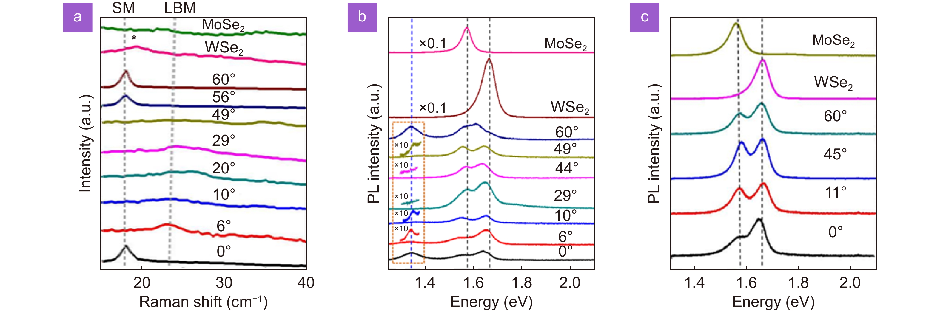
TMD/TMD heterostructure. (a) Low frequency Raman spectra of MoSe2/WSe2 HSs and individual TMD layers with different twist angles (0° ≤ θ ≤ 60°) showing the shear mode (SM), layer-breathing mode (LBM), and unassigned peak (marked with asterisk). The pronounced SM at specific twisting angles indicating the strong coupling of the HS at those angles. (b) PL spectra of the same HS showing the emergence of the interlayer exciton peak at ~ 1.35 eV as a function of different twisting angles. (c) PL spectra of 1L MoSe2, 1L WSe2, and 1L h-BN-inserted HSs with various twist angles (0° ≤ θ ≤ 60°) showing the absence of the interlayer exciton peak at all twisting angles indicating the reduced coupling between MoSe2 and WSe2. The intensity of the main peaks at the HS are comparable to individual layers further indicating the PL spectra is a combination of each individual material in case of no coupling. Figure reproduced with permission from ref.86, Copyright © 2017, American Chemical Society.
-
Figure 3.
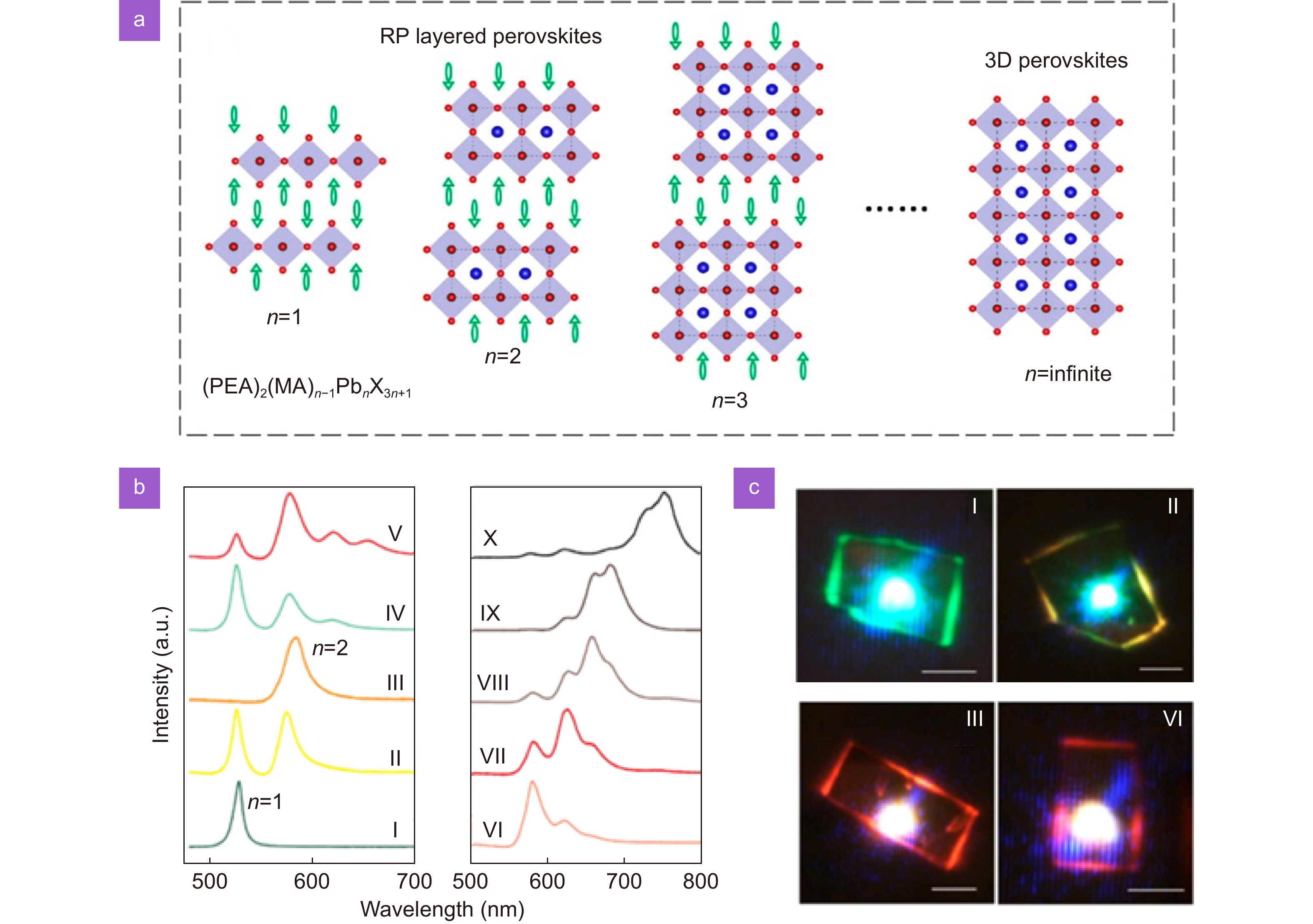
Perovskite/perovskite heterostructure. (a) Schematic crystal structures of (PEA)2(MA)n-1PbnX3n+1 perovskites with different n values. n = ∞ - 3D perovskite. (b) PL spectra of various HSs excited by a 442 nm laser. 527 nm peak corresponds to (PEA)2PbI4 (n = 1), and the 575 nm peak - (PEA)2(MA)Pb2I7 (n = 2). (c) Optical images of different HSs (from Fig.3 (b)) under 442 nm. Scale bars are 5 μm. Figure reproduced with permission from ref.150, Copyright © 2018, American Chemical Society.
-
Figure 4.
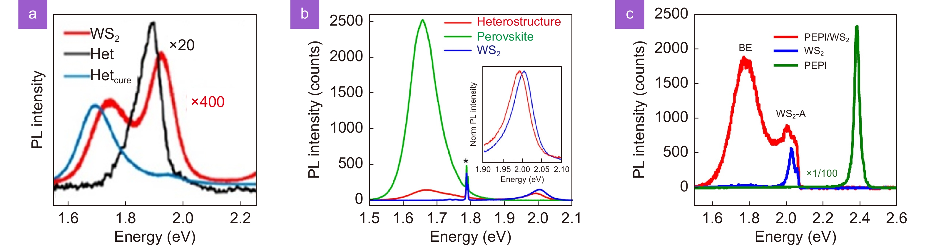
Perovskite/TMD heterostructures. (a) Demonstration of PL enhancement: PL spectra of the 2-layers WS2 (red), and BA2MA3Pb4I13/WS2 heterostructure before (black) and after (blue) interface curing using laser annealing. (b) Demonstration of PL quenching: PL spectra of the monolayer WS2 (blue), MAPbI3 (green), MAPbI3/WS2 heterostructure (red), the insertion highlights the WS2 peak shift due to trion emission. The asterisk (*) indicates the peak from the sapphire substrate. (c) PL spectra of the (C6H5C2H4NH3)2PbI4 (PEPI) perovskite (green), 1L WS2 (blue), broadband emission in the perovskite/WS2 heterostructure (red) originated from the interface interlayer excitons at 110 K. Figure reproduced with permission from: (a) ref.93, Copyright © 2019, American Chemical Society; (b) ref.161, Copyright © 2019, American Chemical Society; (c) ref.95, Copyright © 2020, American Chemical Society.
-
Figure 5.
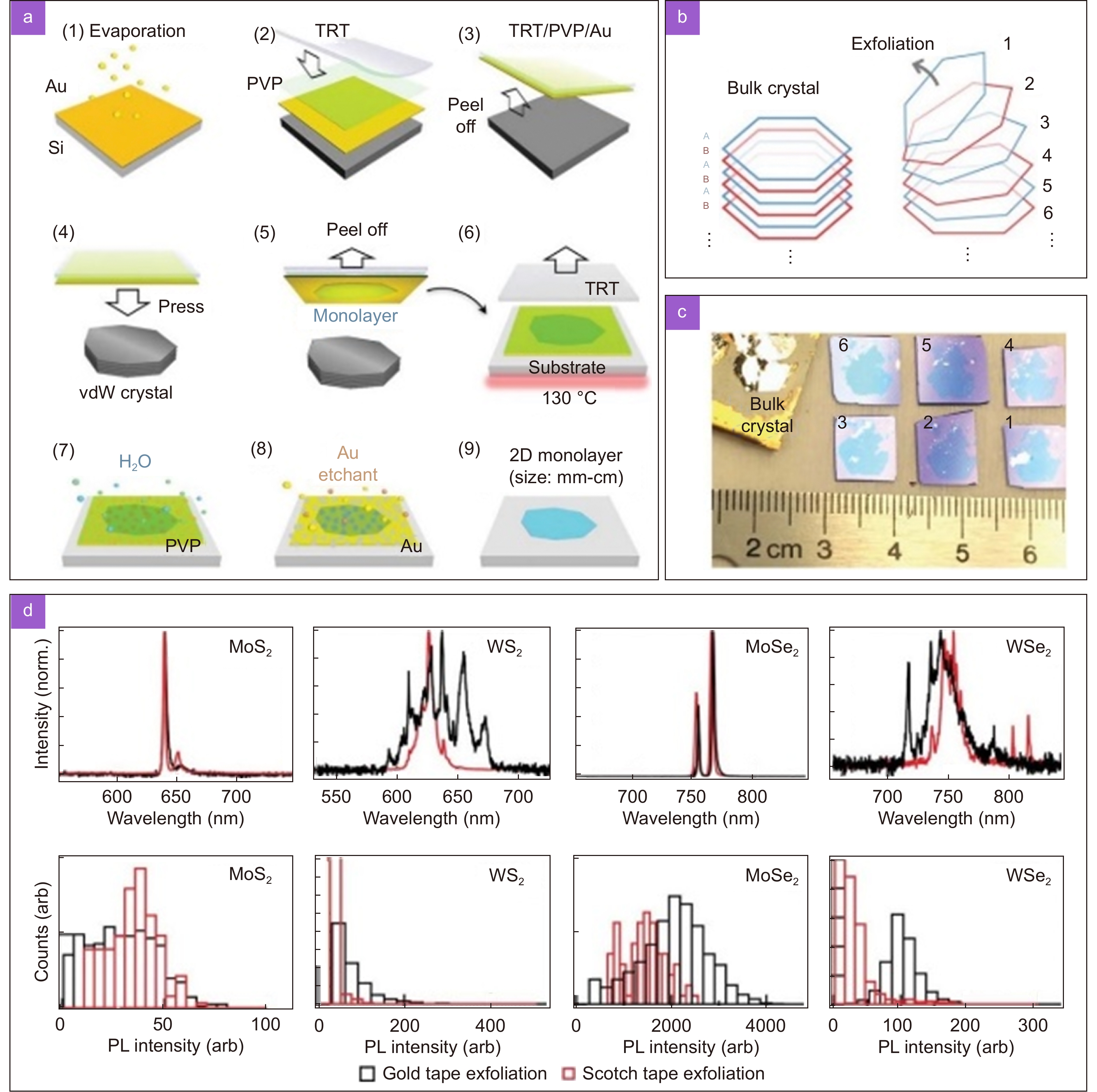
Schematic illustration of Au-assisted exfoliation PL for the large area TMDs monolayers. (a) Steps of large area exfoliation of TMDs using Au (TRT stands for thermal release tape). (b) Schematic of the layer-by-layer exfoliation technique to yield even and odd layers from an AB-stacked vdWs crystal. (c) Photograph for large area monolayers. (d) Comparison of PL spectra of Au-assisted exfoliation and traditional exfoliation measured at 4K for different TMDs (top) and intensity distributions (bottom). Black and red colures for Au and Scotch tape–exfoliation, respectively. Figure reproduced with permission from ref.180, Copyright © 2020, AAAS.
-
Figure 6.
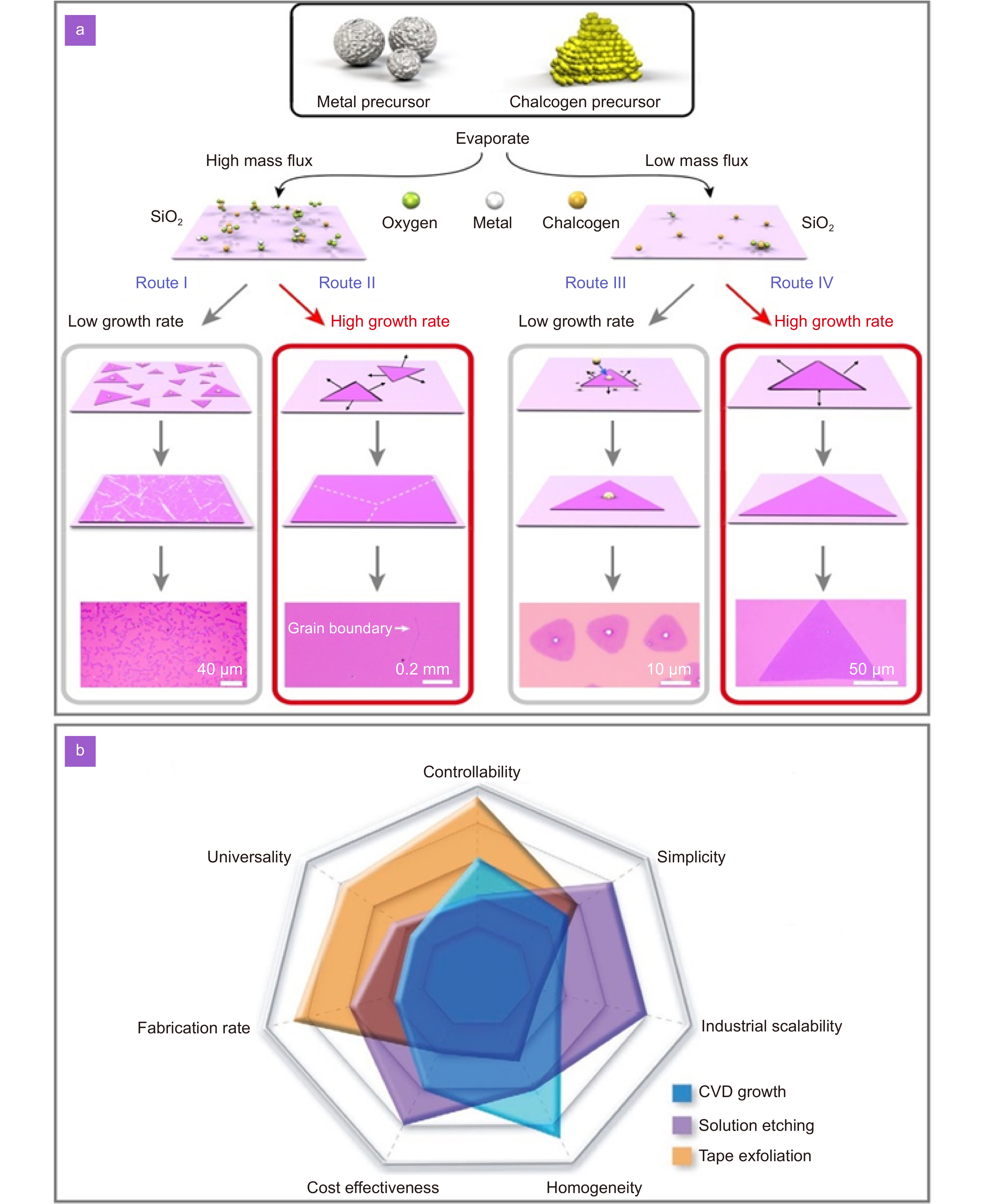
Flow chart for TMDs production via CVD method and comparison with various fabrication strategies for TMDs heterostructures. (a) General growth process to produce TMDs via CVD. (b) Comprehensive comparison of various fabrication strategies of TMDs heterostructures. Figure reproduced with permission from: (a) ref.184. Springer Nature; (b) ref.182. John Wiley and Sons.
-
Figure 7.
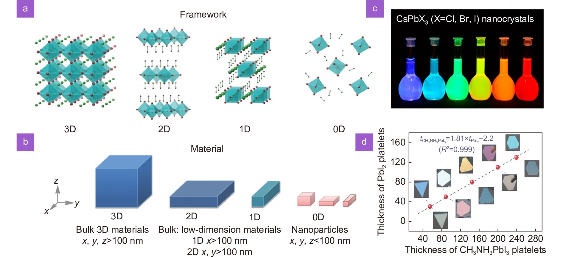
(a) Schematic representation of halide perovskite materials with different dimensionalities ranging from 3D to 0D. (b) Schematic representation of materials with different degrees of confinement. (c) Image of colloidal perovskite nanocrystals taken under UV lamp (λ = 365 nm), which feature tunable emission behavior as a function of composition and particle size. (d) Diagram correlating different thicknesses of PbI2 platelets and the corresponding CH3NH3PbI3 (images below data line) grown on muscovite mica using van der Waals epitaxial growth. Figure reproduced with permission from: (a, b) ref.337, John Wiley and Sons; (c) ref.190, Copyright © 2015, American Chemical Society; (d) ref.188, John Wiley and Sons.
-
Figure 8.
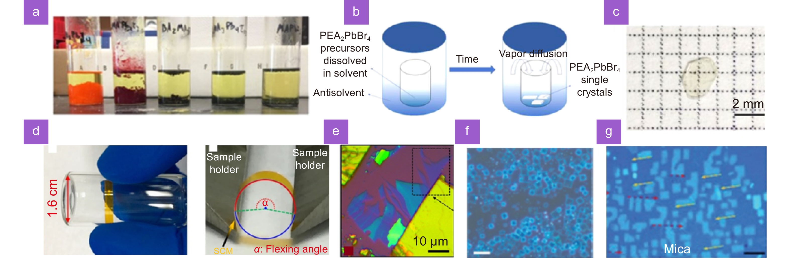
Perovskites synthesized by different methods. (a) Photographs of (CH3(CH2)3NH3)2(CH3NH3)n-1PbnI3n+1 crystallites obtained from acid precipitation method. (b) Schematic illustration of antisolvent vapor-assisted crystallization method. (c) Optical image of (C6H5CH2CH2NH3)2PbBr4 single crystal obtained from the technique. (d) Images of a piece of (C6H5CH2CH2NH3)2PbI4 single crystal grown from induced peripheral crystallization (3.5 μm in thickness) that wrapped around a small tube (1.6 cm in diameter; left), demonstrating its flexibility and was used for a flexing angle study (right). (e) Optical micrograph of exfoliated (C4H9NH3)2PbI4 flakes grown on SiO2/Si substrates. (f) Optical image of atomically thin 2D (C4H9NH3)2PbBr4 obtained from colloidal method with a scale bar of 10 μm. (g) Epitaxial (C4H9NH3)2PbI4 flakes deposited on mica by co-evaporation where the two in-plane orientations were marked by red and orange arrows with an offset θ about 9° (center; scale bar of 5 μm)218. Figure reproduced with permission from: (a) ref.203, Copyright © 2016, American Chemical Society; (b, c) ref.204, Copyright © 2017, American Chemical Society; (d) ref.210, under the terms of the Creative Commons CC BY license; (e) ref.211, American Physical Society; (f) ref.147, AAAS; (g) ref.218, John Wiley and Sons © 2017 WILEY‐VCH Verlag GmbH & Co. KGaA, Weinheim.
-
Figure 9.
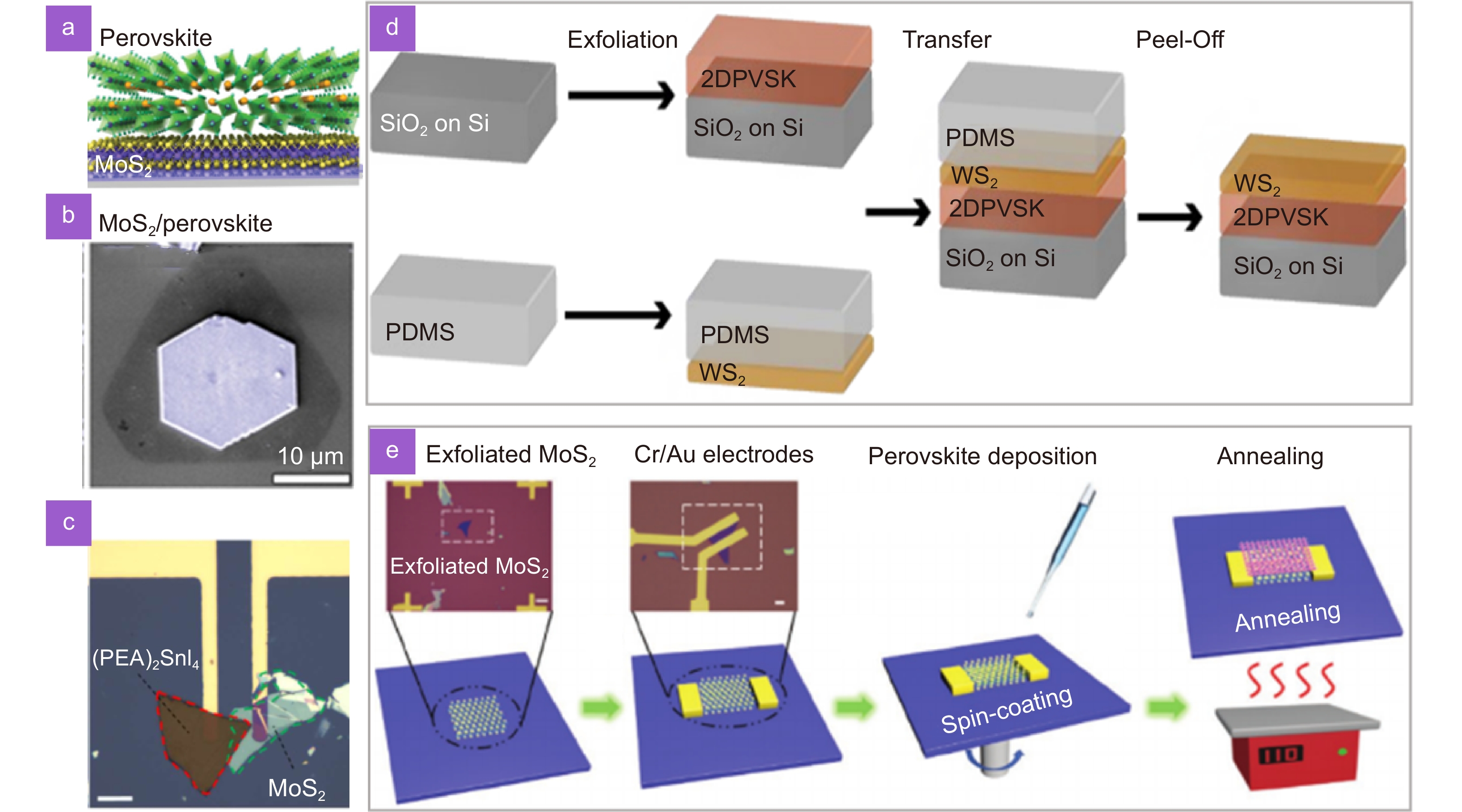
Fabrication of TMD-perovskite heterostructures and devices. (a) Structure models of halide perovskite/MoS2 heterostructure. (b) False-colored scanning electron microscopy image of evaporated perovskite on MoS2 exhibiting triangular and hexagonal shape. (c) Optical microscope image of the as fabricated (PEA)2SnI4/MoS2 PD (the scale bar is 20 μm). (d) Schematics of typical exfoliation and dry transfer process for perovskite/TMD heterostructure fabrication. (e) Schematic diagram of the facile fabrication process of 2D perovskite/TMD heterostructure with spincoating. Figure reproduced with permission from: (a, b) ref.192, John Wiley and Sons; (c) ref.242. Copyright © 2019, American Chemical Society; (d) ref.93. Copyright © 2019, American Chemical Society; (e) ref.158. John Wiley and Sons.
-
Figure 10.
(a) MAPbI3/MoS2/APTES and cross-sectional structure illustration of APTES doping process. (b) Comparison of the photoresponsivity values of MoS2, MoS2/APTES, and perovskite/MoS2/APTES PDs as a function of wavelength. (c) Structure of MAPbI3/WS2 PD on sapphire substrate and the relative type-II band alignment. (d) Spectral responsivity and detectivity of the PD showing its high detectivity. (e) MAPbI3/MoS2 PD with their relative band alignment (left panel) and charge transfer mechanisms (right panel) using 1T and 2H phases of MoS2. (f) Responsivity and detectivity values of MAPbI3/1T-MoS2 PD as a function of illumination powers using 500 nm laser. (g–h) Planar (g), and vertical (h) structures of MAPbI3/MoS2 PDs and the effect of the drain bias and illumination on carrier transportation and separation. (i) I-V curves of the vertical structure under different power densities showing the photovoltaic characteristics of this hybrid structure. Inset is schematic carrier transportation and separation in this self-power mode. Figure reproduced with permission from: (a, b) ref.239, (c, d) ref.163, (e, f) ref.90, (g–i) ref.256, John Wiley and Sons.
-
Figure 11.
(a) MAPbI3/BP/MoS2 and charge transfer mechanism showing both type-I and type-II band alignment at perovskite/BP and BP/MoS2 interfaces, respectively. (b) The temporal response of MAPbI3/BP/MoS2 hybrid PD, inset shows the measured rise and fall times under 457 nm excitation. (c) The temporal response of the PD at zero bias mode under different illumination wavelengths. (d, e) Schematic and relative band diagram of MAPbI3-MoS2 BHJ/rGO PD on SiO2/Si and flexible PEN substrates. (f) Comparison of the photoresponsivity and detectivity values at 660 nm as a function of illumination intensity of the PD with and without using MoS2 on SiO2/Si substrate. Figure reproduced with permission from: (a–c) ref.91. Copyright © 2019, American Chemical Society; (d–f) ref.257, John Wiley and Sons.
-
Figure 12.
(a) Schematic and energy band alignment of CsPbI3-xBrx QDs/MoS2 PD. (b) Photoresponsivity, specific detectivity, and EQE (inset) of CsPbI3-xBrx QDs/MoS2 PD as a function of illumination powers at 532 nm. (c–e) Schematic (c), spectral responsivity and corresponding detectivity (d), and temporal photoresponse at 808 nm excitation (e) of Cs-doped FAPbI3/PtSe2 PD. (f–h) Schematic (f), responsivity and detectivity as a function of illumination intensity at 808 nm (g), and rise/fall times at 808 nm (h) of Cs-doped FAPbI3/PdSe2 hybrid PD. Figures reproduced/adapted with permission from: (a, b) ref.255, under the terms of the Creative Commons Attribution License; (c–e) ref.278, Copyright © 2018, American Chemical Society; (f–h) ref.279, under the terms of the Creative Commons Attribution License.
-
Figure 13.
Summary of performance metrics of perovskite/TMD PDs in comparison with commercial PDs. (a) Current responsivity against response time of perovskite/TMD PDs in comparison with that for the commercial Si and InGaAs. The marked area on the left showing the goal for future development by improving the gain-bandwidth product. (b) Detectivity comparison between perovskite/TMD PDs and commercial Si and InGaAs PDs. The marked area on the right showing the ultimate target for future development through extending the sensitivity range of the PDs to longer wavelength regime which lacks of candidates with suitable bandgap values. The data for perovskite/TMD PDs were taken from the references shown in Table 4.
-
Figure 14.
(a) Representative J-V curve of PSCs with PEDOT: PSS, MoS2, and WS2 as the hole transporting material. (b) Plots of PCEs of PSCs based on PEDOT: PSS, MoS2, and WS2 as the function of the storage time. For each group of measurements, 20 cells were adopted for analysis. (c) The statistic plot for power conversion efficiency of PSCs using different thicknesses of WS2 as the electron transporting material. (d) EQE spectra and integrated current density (J) of the corresponding devices. Figure reproduced with permission from: (a, b) ref.291, Copyright © 2017, American Chemical Society; (c, d) ref.292, John Wiley and Sons.
-
Figure 15.
(a) Schematic diagram of the vdW epitaxial growth of the perovskite crystallizes on a TMD (e.g., WSe2) surface. (b) Energy-band diagram under flat-band conditions of the fabricated planar inverted PSCs with different materials as the HTL. (c) J–V curves the best performing PSCs with and without WS2 interlayer. (d) HRTEM image of one of the MoS2 flakes (synthesized via a solvent-exchange process upon liquid phase exfoliation) oriented in the [001] zone axis having a 2H structure (a sketch of the arrangement of Mo and S atoms in this structure and orientation is superimposed on the HRTEM image). (e) The cross-sectional TEM image of a PSC with 2D MoS2 nanoflakes acting as HTL buffer layer. The scale bar is 1 μm (f) Operational stability of PSCs with and without a MoS2 buffer layer302. Figures reproduced/adapted with permission from: (a) ref.295, under the terms of the Creative Commons Attribution License; (b) ref.289, (c) ref.296, (d) ref.301. John Wiley and Sons; (e, f) ref.302, under a Creative Commons Attribution 4.0 International License.


