
 E-mail Alert
 RSS
RSS
| Citation: |
Ye K T, Li D P, Sun X W, et al. Research progress of quantum dot micro display technology[J]. Opto-Electron Eng, 2022, 49(12): 220008. doi: 10.12086/oee.2022.220008

|
Research progress of quantum dot micro display technology
-
Abstract
The quantum dot is a kind of semiconductor nanocrystal with quantum confinement effect, which attracts a lot of attention due to the excellent optoelectronic properties and has been widely used in the display area. The quantum dot become one of the core materials of display with several advantages including the high luminance efficiency, tunable emission wavelength, narrow FWHM and low-cost solution fabrication. Micro display technology is applied in the near eye display scenario with small effective display area (diagonal < 1 inch). Recently, the rising of VR/AR application scenarios require micro display technology with higher luminance, higher pixel density, and full color display. In this paper, we review the current progress of the quantum dot in micro display from photoluminescence and electroluminescence technique routes. The chances and challenges of the quantum dot in micro display are also summarized.-
Keywords:
- quantum dot /
- micro display /
- photoluminescence /
- electroluminescence
-

-
References
[1] Cheng D W, Wang Q W, Liu Y, et al. Design and manufacture AR head-mounted displays: A review and outlook[J]. Light Adv Manuf, 2021, 2(3): 24. doi: 10.37188/lam.2021.024 [2] Algorri J F, Del Pozo V U, Sańchez-Pena J M, et al. An autostereoscopic device for mobile applications based on a liquid crystal microlens array and an OLED display[J]. J Disp Technol, 2014, 10(9): 713−720. doi: 10.1109/JDT.2014.2313143 [3] Huang Y G, Hsiang E L, Deng M Y, et al. Mini-LED, micro-LED and OLED displays: present status and future perspectives[J]. Light Sci Appl, 2020, 9: 105. doi: 10.1038/s41377-020-0341-9 [4] Lee V W, Twu N, Kymissis I. Micro-LED technologies and applications[J]. Inf Disp, 2016, 32(6): 16−23. [5] Wu T Z, Sher C W, Lin Y, et al. Mini-LED and micro-LED: promising candidates for the next generation display technology[J]. Appl Sci, 2018, 8(9): 1557. doi: 10.3390/app8091557 [6] Huang Y G, Tan G J, Gou F W, et al. Prospects and challenges of mini-LED and micro-LED displays[J]. J Soc Inf Disp, 2019, 27(7): 387−401. doi: 10.1002/jsid.760 [7] Liu Z J, Lin C H, Hyun B R, et al. Micro-light-emitting diodes with quantum dots in display technology[J]. Light Sci Appl, 2020, 9: 83. doi: 10.1038/s41377-020-0268-1 [8] Bera D, Qian L, Tseng T K, et al. Quantum dots and their multimodal applications: a review[J]. Materials, 2010, 3(4): 2260−2345. doi: 10.3390/ma3042260 [9] Vasudevan D, Gaddam R R, Trinchi A, et al. Core–shell quantum dots: properties and applications[J]. J Alloys Compd, 2015, 636: 395−404. doi: 10.1016/j.jallcom.2015.02.102 [10] Dai X L, Deng Y Z, Peng X G, et al. Quantum-dot light-emitting diodes for large-area displays: towards the dawn of commercialization[J]. Adv Mater, 2017, 29(14): 1607022. doi: 10.1002/adma.201607022 [11] Tan Z K, Moghaddam R S, Lai M L, et al. Bright light-emitting diodes based on organometal halide perovskite[J]. Nat Nanotechnol, 2014, 9(9): 687−692. doi: 10.1038/nnano.2014.149 [12] Wang H C, Bao Z, Tsai H Y, et al. Perovskite quantum dots and their application in light-emitting diodes[J]. Small, 2018, 14(1): 1702433. doi: 10.1002/smll.201702433 [13] Van Le Q, Hong K, Jang H W, et al. Halide perovskite quantum dots for light-emitting diodes: properties, synthesis, applications, and outlooks[J]. Adv Electron Mater, 2018, 4(12): 1800335. doi: 10.1002/aelm.201800335 [14] Chen D Q, Chen X. Luminescent perovskite quantum dots: synthesis, microstructures, optical properties and applications[J]. J Mater Chem C, 2019, 7(6): 1413−1446. doi: 10.1039/C8TC05545A [15] Miao Y F, Ke Y, Wang N N, et al. Stable and bright formamidinium-based perovskite light-emitting diodes with high energy conversion efficiency[J]. Nat Commun, 2019, 10(1): 3624. doi: 10.1038/s41467-019-11567-1 [16] Supran G J, Shirasaki Y, Song K W, et al. QLEDs for displays and solid-state lighting[J]. MRS Bull, 2013, 38(9): 703−711. doi: 10.1557/mrs.2013.181 [17] Zhu R D, Luo Z Y, Chen H W, et al. Realizing Rec. 2020 color gamut with quantum dot displays[J]. Opt Express, 2015, 23(18): 23680−23693. doi: 10.1364/OE.23.023680 [18] Liu Z J, Hyun B R, Sheng Y J, et al. Micro-light-emitting diodes based on InGaN materials with quantum dots[J]. Adv Mater Technol, 2022, 7(6): 2101189. doi: 10.1002/admt.202101189 [19] Fan X T, Wu T Z, Liu B, et al. Recent developments of quantum dot based micro-LED based on non-radiative energy transfer mechanism[J]. Opto-Electron Adv, 2021, 4(4): 210022. doi: 10.29026/oea.2021.210022 [20] Nasirzadeh K, Nazarian S, Hayat S M G. Inorganic nanomaterials: a brief overview of the applications and developments in sensing and drug delivery[J]. J Appl Biotechnol Rep, 2016, 3(2): 395−402. [21] Green M A, Ho-Baillie A, Snaith H J. The emergence of perovskite solar cells[J]. Nat Photonics, 2014, 8(7): 506−514. doi: 10.1038/nphoton.2014.134 [22] Hong N H. Introduction to nanomaterials: basic properties, synthesis, and characterization[M]//Hong N H. Nano-Sized Multifunctional Materials. Amsterdam: Elsevier, 2019: 1–19. [23] Feng F, Zhang K, Liu Y B, et al. AlGaN-based deep-UV micro-LED array for quantum dots converted display with ultra-wide color gamut[J]. IEEE Electron Device Lett, 2022, 43(1): 60−63. doi: 10.1109/LED.2021.3130750 [24] Singh M, Haverinen H M, Dhagat P, et al. Inkjet printing-process and its applications[J]. Adv Mater, 2010, 22(6): 673−685. doi: 10.1002/adma.200901141 [25] Lan L H, Zou J H, Jiang C B, et al. Inkjet printing for electroluminescent devices: emissive materials, film formation, and display prototypes[J]. Front Optoelectron, 2017, 10(4): 329−352. doi: 10.1007/s12200-017-0765-x [26] Liu Y, Li F S, Xu Z W, et al. Efficient all-solution processed quantum dot light emitting diodes based on inkjet printing technique[J]. ACS Appl Mater Interfaces, 2017, 9(30): 25506−25512. doi: 10.1021/acsami.7b05381 [27] Yang P H, Zhang L, Kang D J, et al. High-resolution inkjet printing of quantum dot light-emitting microdiode arrays[J]. Adv Opt Mater, 2020, 8(1): 1901429. doi: 10.1002/adom.201901429 [28] Hu Z P, Yin Y M, Ali M U, et al. Inkjet printed uniform quantum dots as color conversion layers for full-color OLED displays[J]. Nanoscale, 2020, 12(3): 2103−2110. doi: 10.1039/C9NR09086J [29] Zheng C B, Zheng X, Feng C, et al. High-brightness perovskite quantum dot light-emitting devices using inkjet printing[J]. Org Electron, 2021, 93: 106168. doi: 10.1016/j.orgel.2021.106168 [30] Han H V, Lin H Y, Lin C C, et al. Resonant-enhanced full-color emission of quantum-dot-based micro LED display technology[J]. Opt Express, 2015, 23(25): 32504−32515. doi: 10.1364/OE.23.032504 [31] Lin H Y, Sher C W, Hsieh D H, et al. Optical cross-talk reduction in a quantum-dot-based full-color micro-light-emitting-diode display by a lithographic-fabricated photoresist mold[J]. Photonics Res, 2017, 5(5): 411−416. doi: 10.1364/PRJ.5.000411 [32] Li Y, Chen Z W, Liang D, et al. Coffee-stain-free perovskite film for efficient printed light-emitting diode[J]. Adv Opt Mater, 2021, 9(17): 2100553. doi: 10.1002/adom.202100553 [33] Gao A J, Yan J, Wang Z J, et al. Printable CsPbBr3 perovskite quantum dot ink for coffee ring-free fluorescent microarrays using inkjet printing[J]. Nanoscale, 2020, 12(4): 2569−2577. doi: 10.1039/C9NR09651E [34] Chen S W H, Shen C C, Wu T Z, et al. Full-color monolithic hybrid quantum dot nanoring micro light-emitting diodes with improved efficiency using atomic layer deposition and nonradiative resonant energy transfer[J]. Photonics Res, 2019, 7(4): 416−422. doi: 10.1364/PRJ.7.000416 [35] Li H G, Duan Y Q, Shao Z L, et al. High-resolution pixelated light emitting diodes based on electrohydrodynamic printing and coffee-ring-free quantum dot film[J]. Adv Mater Technol, 2020, 5(10): 2000401. doi: 10.1002/admt.202000401 [36] Park J S, Kyhm J, Kim H H, et al. Alternative patterning process for realization of large-area, full-color, active quantum dot display[J]. Nano Lett, 2016, 16(11): 6946−6953. doi: 10.1021/acs.nanolett.6b03007 [37] Mei W H, Zhang Z Q, Zhang A D, et al. High-resolution, full-color quantum dot light-emitting diode display fabricated via photolithography approach[J]. Nano Res, 2020, 13(9): 2485−2491. doi: 10.1007/s12274-020-2883-9 [38] Kim H M, Ryu M, Cha J H J, et al. Ten micrometer pixel, quantum dots color conversion layer for high resolution and full color active matrix micro-LED display[J]. J Soc Inf Disp, 2019, 27(6): 347−353. doi: 10.1002/jsid.782 [39] Li X H, Kundaliya D, Tan Z J, et al. Projection lithography patterned high-resolution quantum dots/thiol-ene photo-polymer pixels for color down conversion[J]. Opt Express, 2019, 27(21): 30864−30874. doi: 10.1364/OE.27.030864 [40] Zhao B X, Zhang X L, Bai X, et al. Surface modification toward luminescent and stable silica-coated quantum dots color filter[J]. Sci China Mater, 2019, 62(10): 1463−1469. doi: 10.1007/s40843-019-9435-7 [41] Cho H, Pan J A, Wu H Q, et al. Direct optical patterning of quantum dot light-emitting diodes via in situ ligand exchange[J]. Adv Mater, 2020, 32(46): 2003805. doi: 10.1002/adma.202003805 [42] Yang J, Hahm D, Kim K, et al. High-resolution patterning of colloidal quantum dots via non-destructive, light-driven ligand crosslinking[J]. Nat Commun, 2020, 11(1): 2874. doi: 10.1038/s41467-020-16652-4 [43] Zhao J Y, Chen L X, Li D Z, et al. Large-area patterning of full-color quantum dot arrays beyond 1000 pixels per inch by selective electrophoretic deposition[J]. Nat Commun, 2021, 12(1): 4603. doi: 10.1038/s41467-021-24931-x [44] Li Y, Tao J, Wang Q, et al. Microfluidics-based quantum dot color conversion layers for full-color micro-LED display[J]. Appl Phys Lett, 2021, 118(17): 173501. doi: 10.1063/5.0047854 [45] Protesescu L, Yakunin S, Bodnarchuk M I, et al. Nanocrystals of cesium lead halide perovskites (CsPbX3, X = Cl, Br, and I): novel optoelectronic materials showing bright emission with wide color gamut[J]. Nano Lett, 2015, 15(6): 3692−3696. doi: 10.1021/nl5048779 [46] Stoumpos C C, Kanatzidis M G. Halide perovskites: poor man's high-performance semiconductors[J]. Adv Mater, 2016, 28(28): 5778−5793. doi: 10.1002/adma.201600265 [47] Veldhuis S A, Boix P P, Yantara N, et al. Perovskite materials for light-emitting diodes and lasers[J]. Adv Mater, 2016, 28(32): 6804−6834. doi: 10.1002/adma.201600669 [48] Li Z T, Cao K, Li J S, et al. Review of blue perovskite light emitting diodes with optimization strategies for perovskite film and device structure[J]. Opto-Electron Adv, 2021, 4(2): 200019. doi: 10.29026/oea.2021.200019 [49] Shi L F, Meng L H, Jiang F, et al. In situ inkjet printing strategy for fabricating perovskite quantum dot patterns[J]. Adv Funct Mater, 2019, 29(37): 1903648. doi: 10.1002/adfm.201903648 [50] Zhan W J, Meng L H, Shao C D, et al. In situ patterning perovskite quantum dots by direct laser writing fabrication[J]. ACS Photonics, 2021, 8(3): 765−770. doi: 10.1021/acsphotonics.1c00118 [51] Jia S Q, Li G Y, Liu P, et al. Highly luminescent and stable green quasi-2D perovskite-embedded polymer sheets by inkjet printing[J]. Adv Funct Mater, 2020, 30(24): 1910817. doi: 10.1002/adfm.201910817 [52] Huang X J, Guo Q Y, Yang D D, et al. Reversible 3D laser printing of perovskite quantum dots inside a transparent medium[J]. Nat Photonics, 2020, 14(2): 82−88. doi: 10.1038/s41566-019-0538-8 [53] Sun K, Tan D Z, Fang X Y, et al. Three-dimensional direct lithography of stable perovskite nanocrystals in glass[J]. Science, 2022, 375(6578): 307−310. doi: 10.1126/science.abj2691 [54] Moon H, Lee C, Lee W, et al. Stability of quantum dots, quantum dot films, and quantum dot light-emitting diodes for display applications[J]. Adv Mater, 2019, 31(34): 1804294. doi: 10.1002/adma.201804294 [55] Chang J H, Park P, Jung H, et al. Unraveling the origin of operational instability of quantum dot based light-emitting diodes[J]. ACS Nano, 2018, 12(10): 10231−10239. doi: 10.1021/acsnano.8b03386 [56] Chen S, Cao W R, Liu T L, et al. On the degradation mechanisms of quantum-dot light-emitting diodes[J]. Nat Commun, 2019, 10(1): 765. doi: 10.1038/s41467-019-08749-2 [57] Rhee S, Kim K, Roh J, et al. Recent progress in high-luminance quantum dot light-emitting diodes[J]. Curr Opt Photonics, 2020, 4(3): 161−173. [58] Sun Y Z, Su Q, Zhang H, et al. Investigation on thermally induced efficiency roll-off: toward efficient and ultrabright quantum-dot light-emitting diodes[J]. ACS Nano, 2019, 13(10): 11433−11442. doi: 10.1021/acsnano.9b04879 [59] Jia S Q, Tang H D, Ma J R, et al. High performance inkjet-printed quantum-dot light-emitting diodes with high operational stability[J]. Adv Opt Mater, 2021, 9(22): 2101069. doi: 10.1002/adom.202101069 [60] Kim T H, Cho K S, Lee E K, et al. Full-colour quantum dot displays fabricated by transfer printing[J]. Nat Photonics, 2011, 5(3): 176−182. doi: 10.1038/nphoton.2011.12 [61] Nam T W, Kim M, Wang Y M, et al. Thermodynamic-driven polychromatic quantum dot patterning for light-emitting diodes beyond eye-limiting resolution[J]. Nat Commun, 2020, 11(1): 3040. doi: 10.1038/s41467-020-16865-7 [62] Meng T T, Zheng Y T, Zhao D L, et al. Ultrahigh-resolution quantum-dot light-emitting diodes[J]. Nat Photonics, 2022, 16(4): 297−303. doi: 10.1038/s41566-022-00960-w [63] Tokito S, Tsutsui T, Taga Y. Microcavity organic light-emitting diodes for strongly directed pure red, green, and blue emissions[J]. J Appl Phys, 1999, 86(5): 2407−2411. doi: 10.1063/1.371068 [64] Genco A, Giordano G, Carallo S, et al. High quality factor microcavity OLED employing metal-free electrically active Bragg mirrors[J]. Org Electron, 2018, 62: 174−180. doi: 10.1016/j.orgel.2018.07.034 [65] Wang M S, Lin J, Hsiao Y C, et al. Investigating underlying mechanism in spectral narrowing phenomenon induced by microcavity in organic light emitting diodes[J]. Nat Commun, 2019, 10(1): 1614. doi: 10.1038/s41467-019-09585-0 [66] Chen L N, Qin Z Y, Chen S M. Ultrahigh resolution pixelated top-emitting quantum-dot light-emitting diodes enabled by color-converting cavities[J]. Small Methods, 2022, 6(1): 2101090. doi: 10.1002/smtd.202101090 [67] Joo W J, Kyoung J, Esfandyarpour M, et al. Metasurface-driven OLED displays beyond 10, 000 pixels per inch[J]. Science, 2020, 370(6515): 459−463. doi: 10.1126/science.abc8530 [68] Wu L J, Liu W Y, Lu Z Z, et al. 72-1: Invited Paper: realizing long lifetime blue quantum dots light emitting diodes (QLEDs) through quantum dot structure tailoring[J]. SID Symp Dig Tech Pap, 2020, 51(1): 1071−1074. doi: 10.1002/sdtp.14059 [69] Won Y H, Cho O, Kim T, et al. Highly efficient and stable InP/ZnSe/ZnS quantum dot light-emitting diodes[J]. Nature, 2019, 575(7784): 634−638. doi: 10.1038/s41586-019-1771-5 [70] Kim T, Kim K H, Kim S, et al. Efficient and stable blue quantum dot light-emitting diode[J]. Nature, 2020, 586(7829): 385−389. doi: 10.1038/s41586-020-2791-x [71] Chao W C, Chiang T H, Liu Y C, et al. High efficiency green InP quantum dot light-emitting diodes by balancing electron and hole mobility[J]. Commun Mater, 2021, 2(1): 96. doi: 10.1038/s43246-021-00203-5 -
Overview
Quantum dot is a kind of semiconductor nanocrystal with a quantum confinement effect. Recently, quantum dots have been applied for display due to their advantages including high photoluminescent efficiency, tunable emission wavelength, narrow emission spectrum, and low-cost solution process. In this paper, we focus on the application of quantum dots in microdisplay. With the rising near-eye display demands such as AR/VR, the realization of full color, high efficiency, and high luminance microdisplay attracts many attentions. However, the realization of the target microdisplay is difficult due to the high-cost mass transfer technology in micro-LED and the insufficient luminance in micro-OLED. Here, the photoluminescent (PL) and electroluminescent (EL) quantum dots can provide new routes for microdisplay. For PL, quantum dots can work as color conversion material for micro-LED. The multiple-time mass transfer can be avoided with the combination of red and green quantum dots and blue micro-LED. Meanwhile, the color gamut can be improved due to the narrow FWHM of quantum dot emission. For EL, RGB quantum dots can work as an emission layer in QLED, and the RGB micro-QLED can be applied for microdisplay directly with a compact and high-efficiency system. Compared with OLED, the QLED can realize higher luminance due to the inherent stability of the inorganic quantum dot, which is more suitable for AR display requiring high luminance. The patterning of quantum dot layer is the first step for the application in microdisplay. For both PL and EL applications, a high pixel density, high pixel uniformity, high pixel consistency, and low-cost patterning method is required. For the quantum dot color conversion layer in PL application, a high optical density is required for the sufficient absorption of the blue light. For the quantum dot emission layer in EL application, the uniform and small roughness surface quantum dot layer is required with few damages to the quantum dots to ensure the good performance of QLED devices. There are several patterning methods have been reported for quantum dots including inkjet printing, photolithography, transfer printing, electrophoretic deposition, in situ fabrication, and optical micro cavity. However, it is still challenging to find a perfect patterning method for the quantum dot layer. For PL application, the stability of quantum dot under long time high-intensity blue light excitation is a big problem due to the photoinduced quenching and oxidation. For EL application, compared with red and green QLED, the peak luminance, efficiency, and lifetime of blue QLED needs to be further improved by optimizing the blue quantum dots and device structure to satisfy the requirement of the display application.
-
Access History
Figures(17)
Tables(1)
Article Metrics

Export File
Citation
Ye K T, Li D P, Sun X W, et al. Research progress of quantum dot micro display technology[J]. Opto-Electron Eng, 2022, 49(12): 220008. doi: 10.12086/oee.2022.220008
Format
Content
 DownLoad:


-
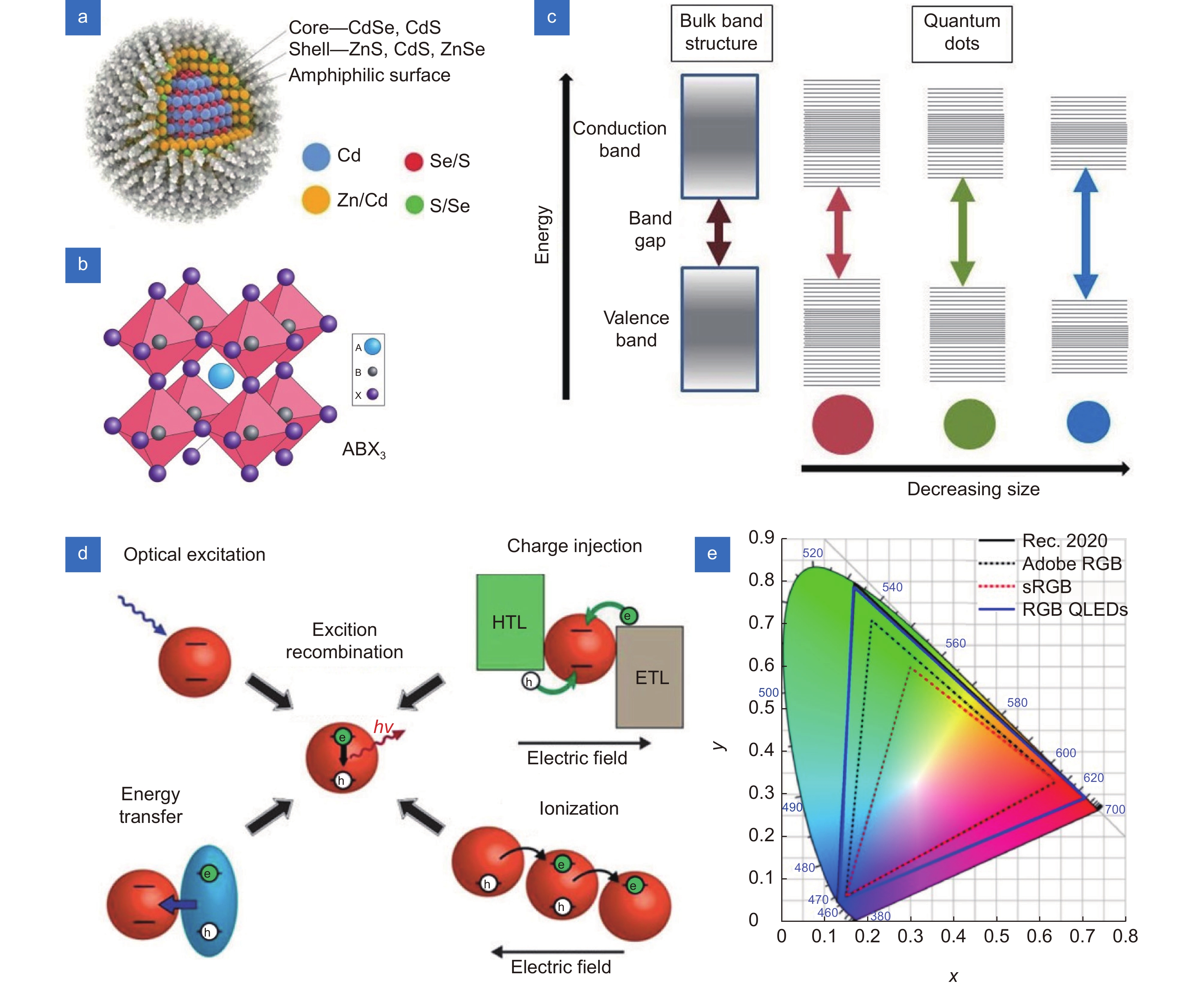
Figure 1.
(a) Core-shell structure diagram of the colloidal quantum dot[20]; (b) Structure diagram of perovskite nanocrystal[21]; (c) Relationship between quantum dot size and emission bandgap[22]; (d) Excitation mechanisms of quantum dots[16]; (e) Color gamut representation of RGB QLEDs[17]
-
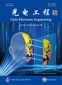
Figure 2.
(a) The schematic diagram of the aerosol jet printing; (b) Full color quantum dots based Micro-LED image under fluorescence microscopy[30]; (c) The process of the full-color emission quantum dots based Micro-LED by aerosol jet printing[31]
-
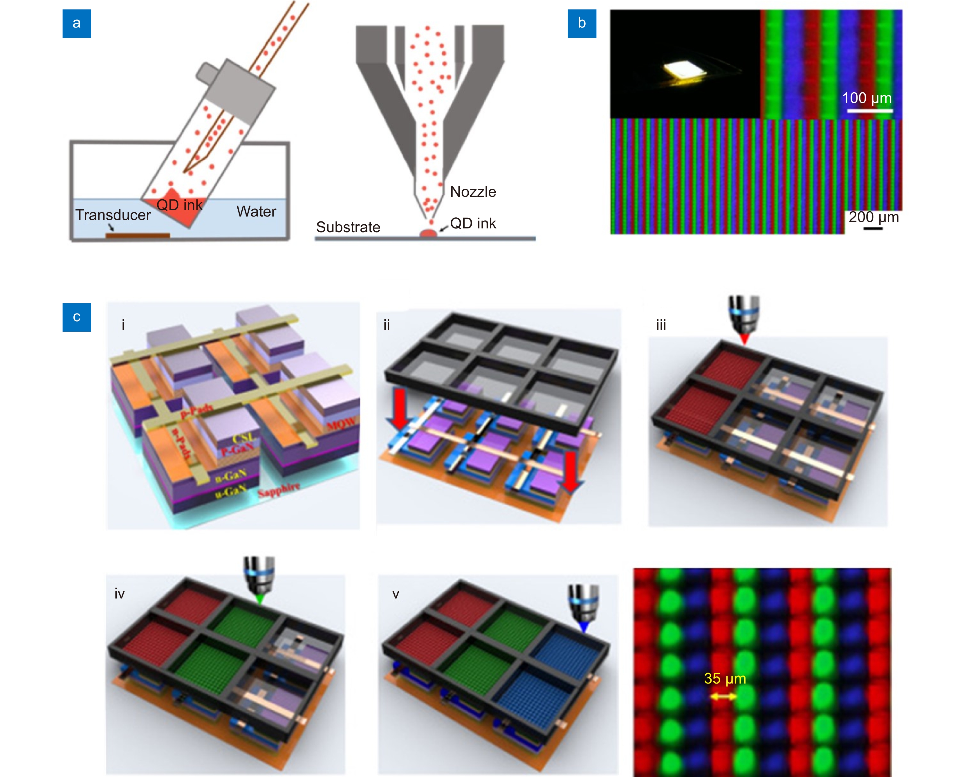
Figure 3.
(a) Schematic illustration of the marangoni flow and capillary flow: surface tension at the top area of the droplet is smaller than the edge(Δγ<0), and surface tension at the top of the droplet is larger than the edge area(Δγ>0); (b) Fluorescence image and corresponding surface profiles of the microarray with dodecane volume ratio of 60%, 70%, and 80% in the ink. The scale bars are 100 μm; (c) A CsPbBr3 quantum dot pattern by inkjet printing[33]
-
Figure 4.
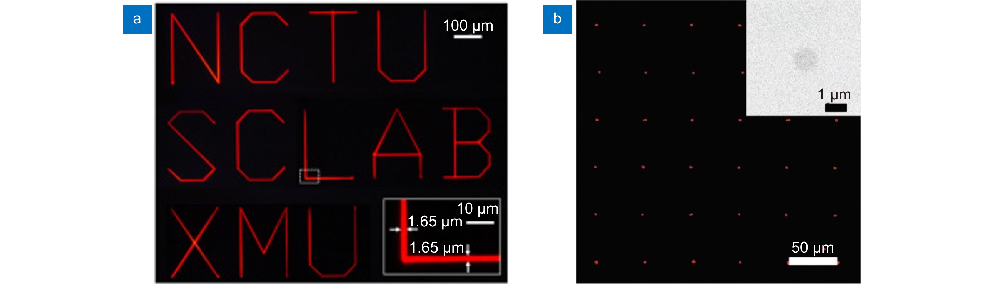
(a) Fluorescence microscope image of patterns printed on the glass by super-inkjet printing system, the minimum linewidth is 1.65 μm[34]; (b) Red quantum dot pattern by electrohydrodynamic printing with a diameter of 1 μm[35]
-
Figure 5.
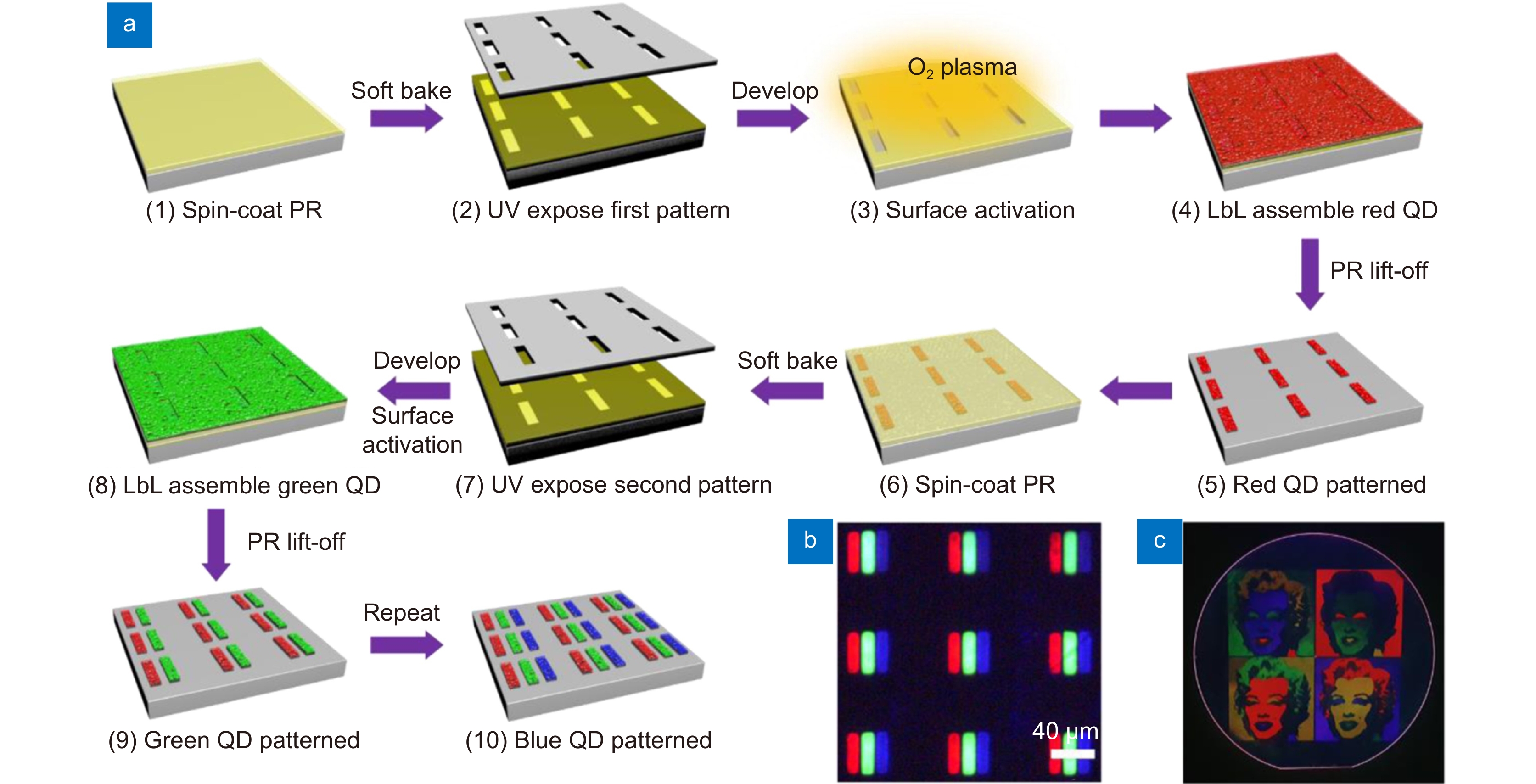
(a) Illustration of the quantum dot patterning by using repeated photolithography; (b) Microscope image of the patterned quantum dot under 405 nm laser excitation; (c) Large-scale quantum dot pattern demonstration on a 4 inch quartz wafer under UV lamp[36]
-
Figure 6.
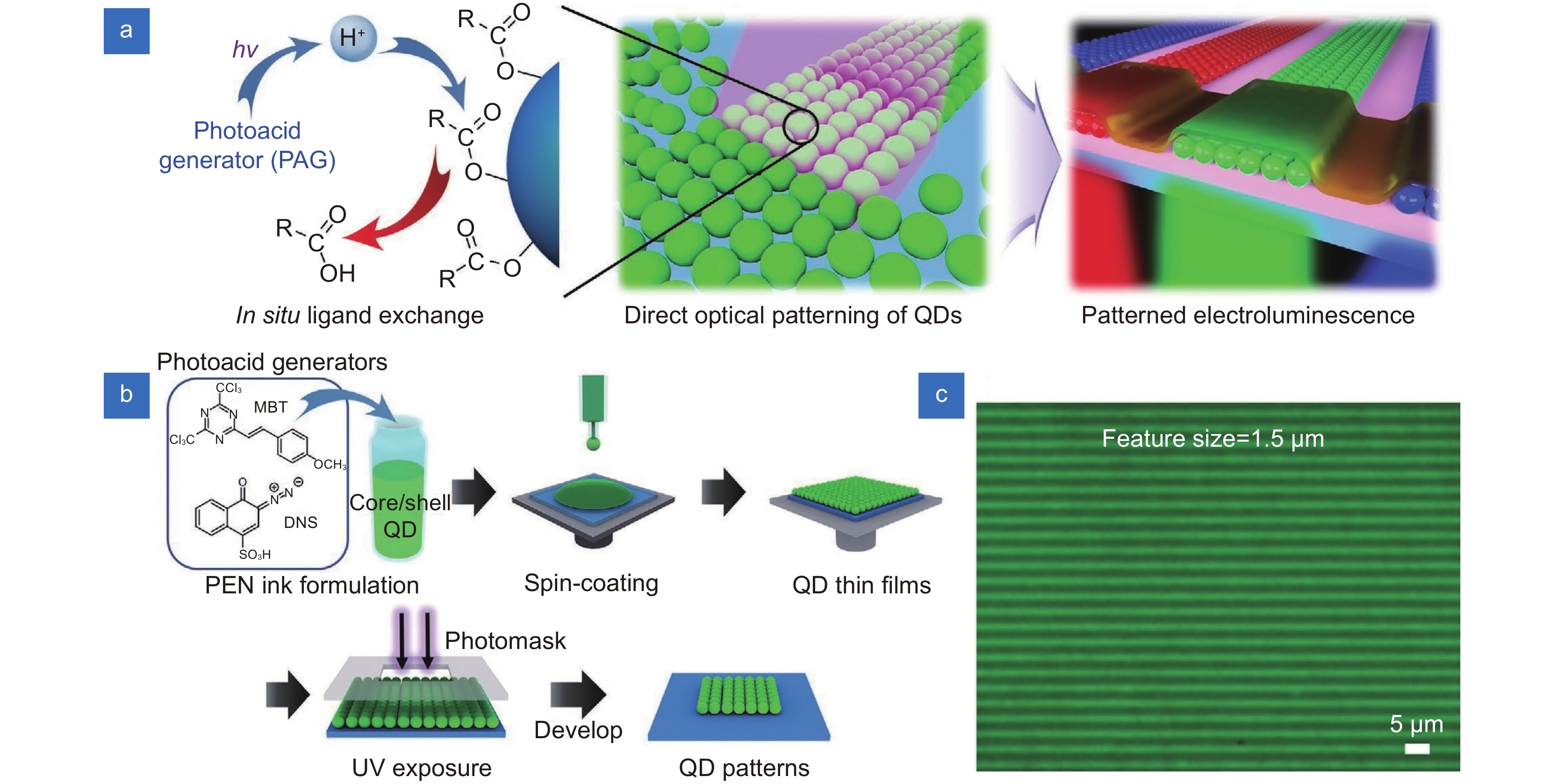
(a) Schematic illustrations of the patterning concept of direct optical lithography of quantum dot; (b) Process of using photo-patternable emissive nanocrystal inks for patterning luminescent quantum dots; (c) Fluorescence optical microscopy images of green quantum dots pattern with a minimum line width of 1.5 μm[41]
-
Figure 7.
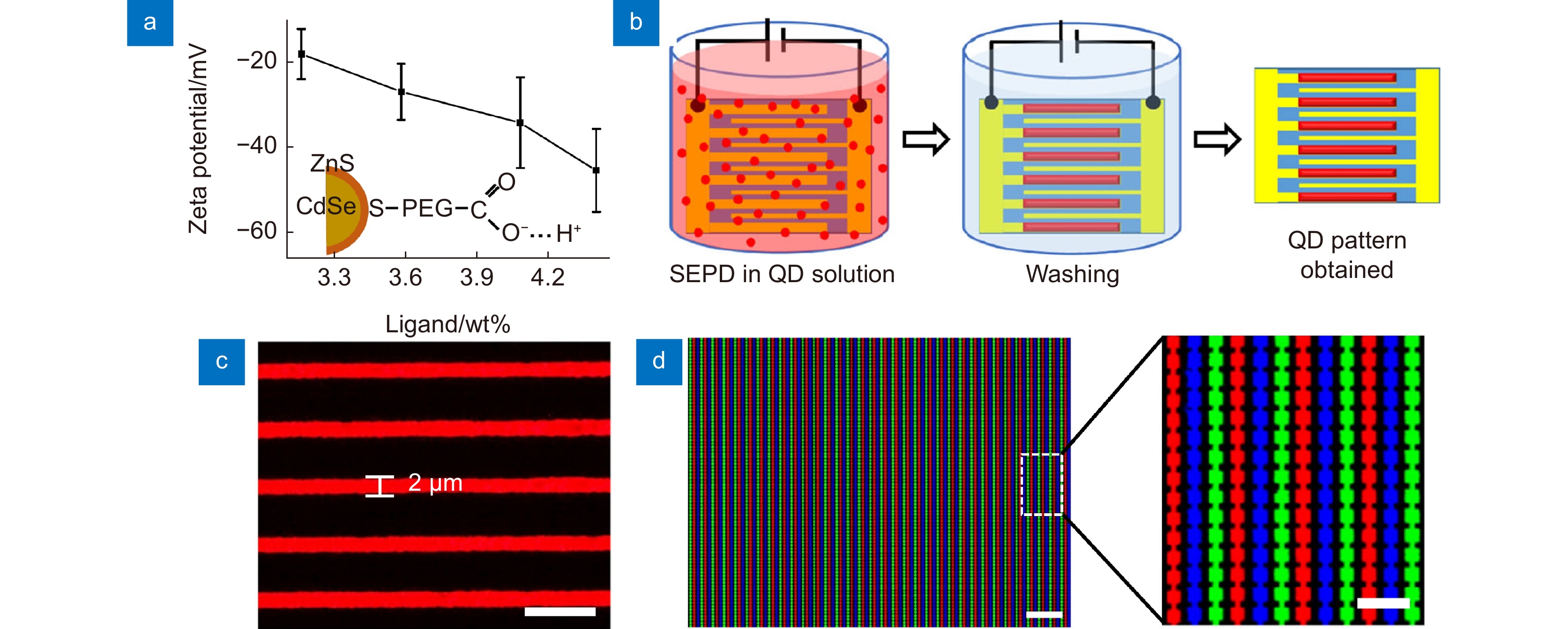
(a) Zeta potentials of quantum dots capped with different ligand contents; (b) Schematic illustration of the quantum dots patterning process on the prefabricated substrate; (c) Fluorescence image of the red quantum dot stripe array with a line width of 2 μm. Scale bar: 10 μm; (d) Fluorescence images of RGB quantum dot patterns fabricated by three steps selective electrophoretic deposition. Scale bar: 200 μm(left) and 50 μm(right)[43]
-
Figure 8.
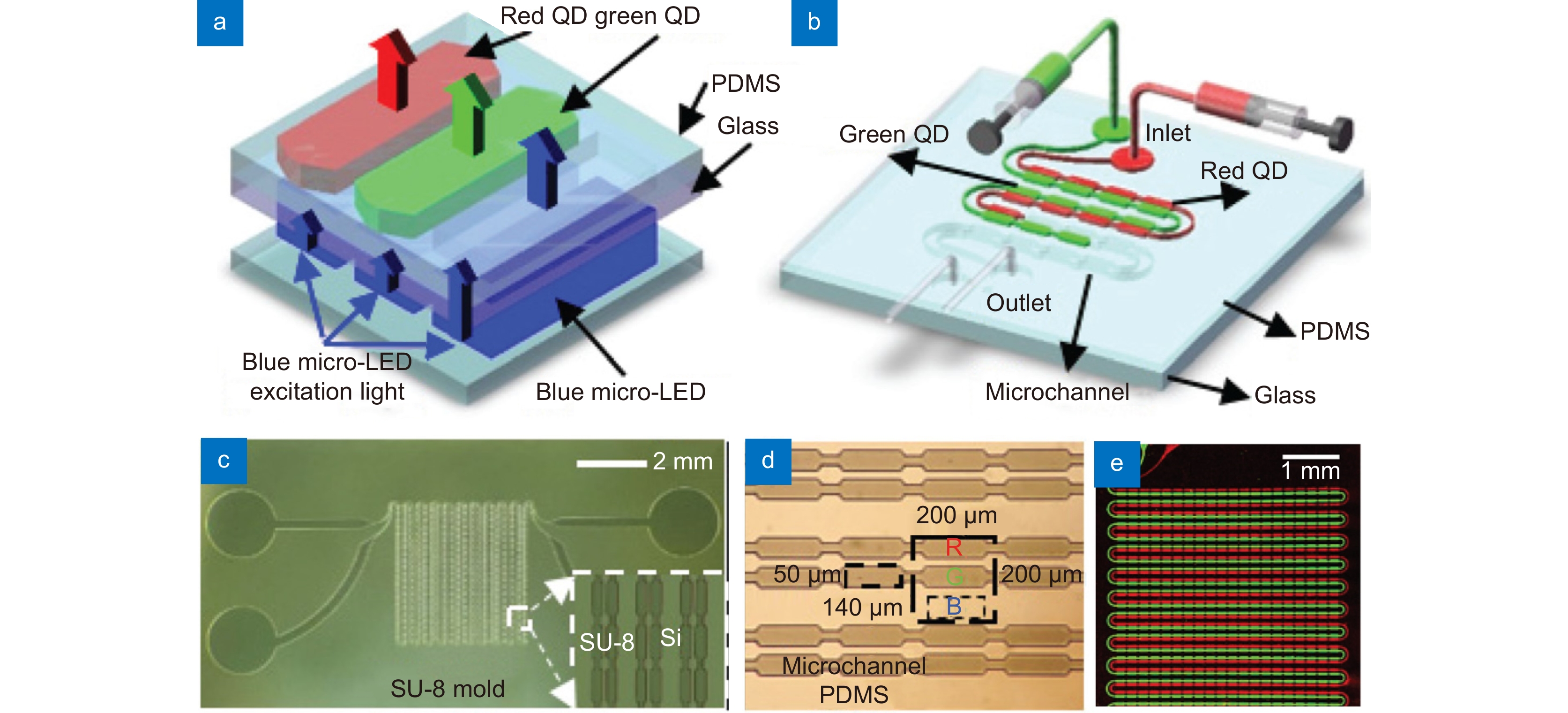
(a) Schematic diagram of a single pixel of the full color Micro-LED display based on red and green quantum dots; (b) Process of red and green quantum dots injection in the micro-channels; (c) SU-8 mold on the silicon substrate; (d) PDMS microchannel bond with the glass substrate with a sub pixel of 50 μm×140 μm; (e) Quantum dot color conversion layer with 200 μm full-color pixel pitches array[44]
-
Figure 9.
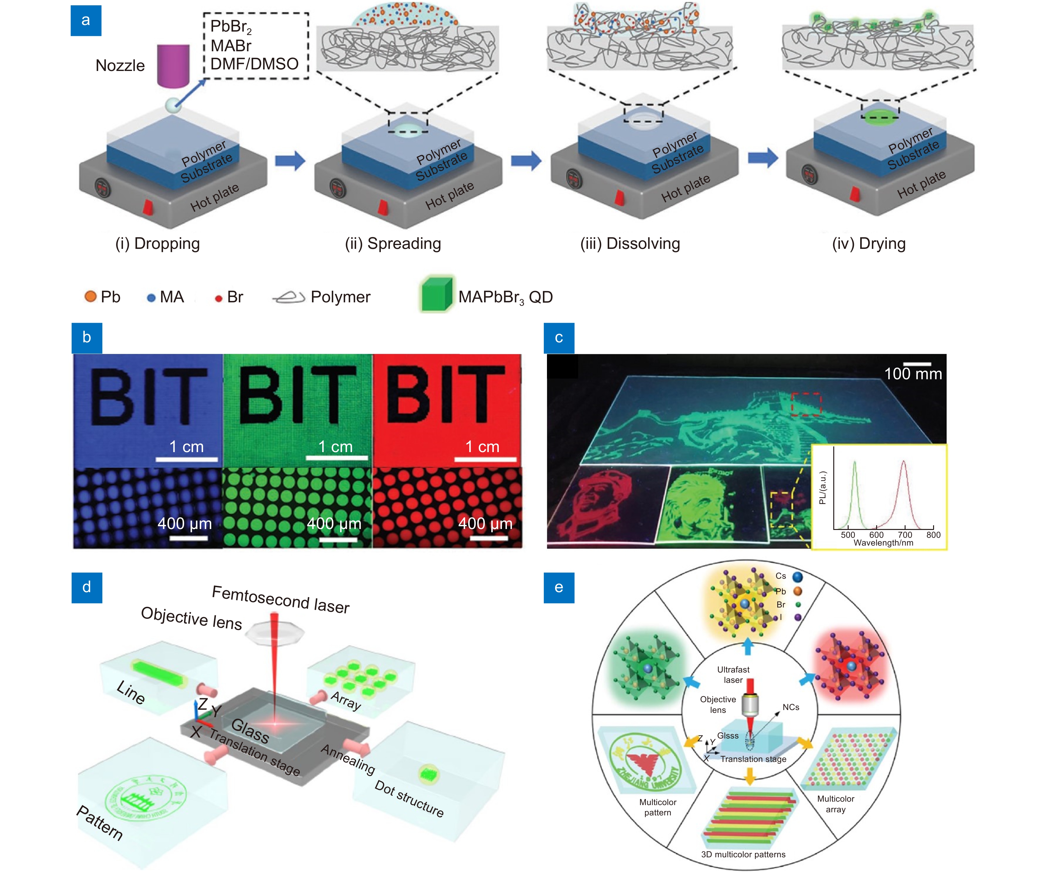
(a) Schematic diagram of in situ inkjet printing strategy for fabricating patterning perovskite quantum dots patterns on polymer substrate; (b) Printed RGB perovskite quantum dots patterns under UV light illuminations[49]; (c) Photography of patterned perovskite-polymer composite sheets[51]; (d) In situ direct laser writing fabrication of perovskite quantum dots patterns inside of the glass[52]; (e) In situ direct laser writing fabrication of perovskite quantum dots with different colors inside of the glass[53]
-
Figure 10.
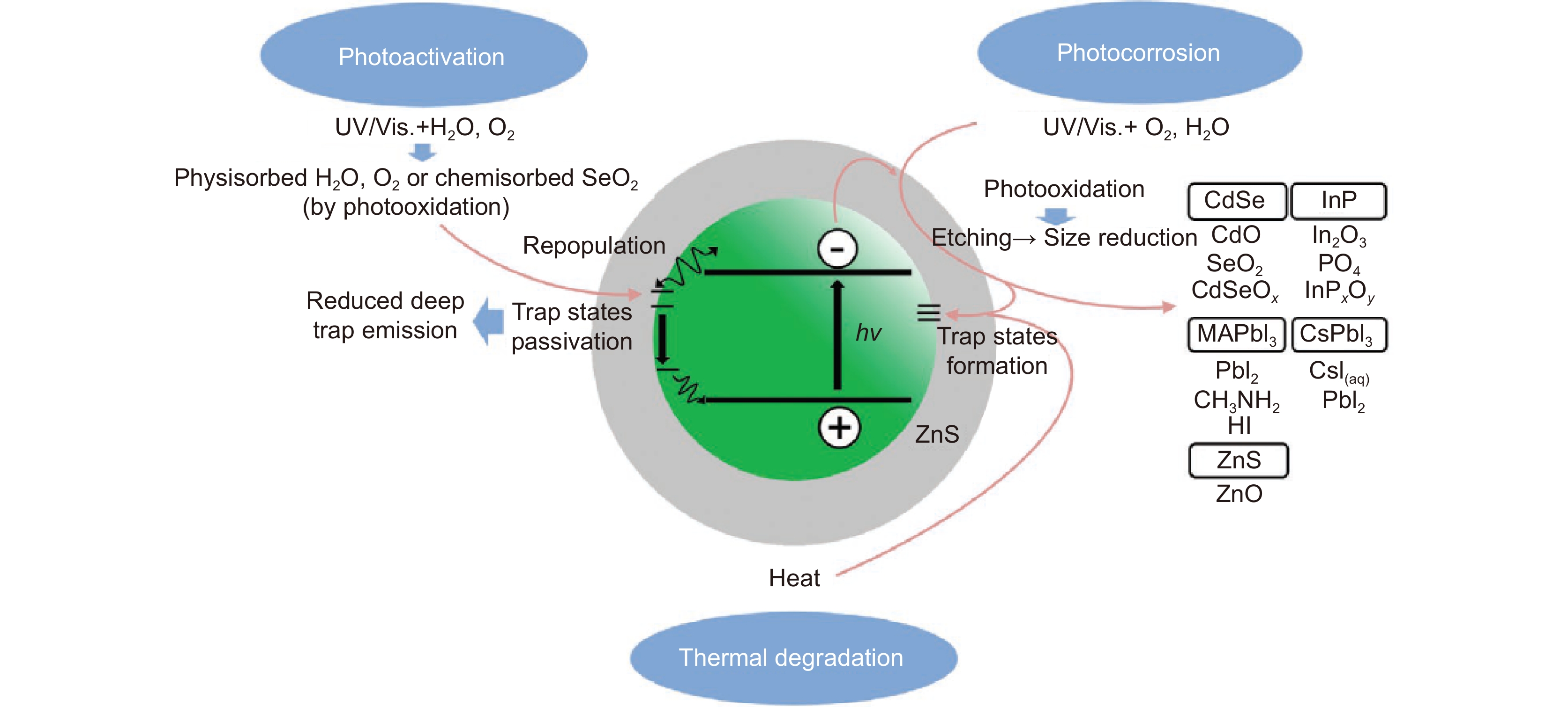
Representative mechanisms for the instability of QDs, including photoactivation, photocorrosion, and thermal degradation[54]
-
Figure 11.
(a) Structure design of the QLED devices; (b) Energy level diagram of the QLED; (c) Schematic of electrohydrodynamic printing to fill the pixel on the substrate[35]; (d) The fluorescent microphotograph of high-resolution pixels by electrohydrodynamic printing; (e) The scheme of droplet evaporation processes for heat post-treatment (HP) and gradient vacuum post-treatment (GVP) methods. EQE-luminance curves of (f) red, (g) green, and (h) blue inkjet printing(circle) and spin-coating(square) QLED. The scale bar is 5 cm in the insert picture[49]
-
Figure 12.
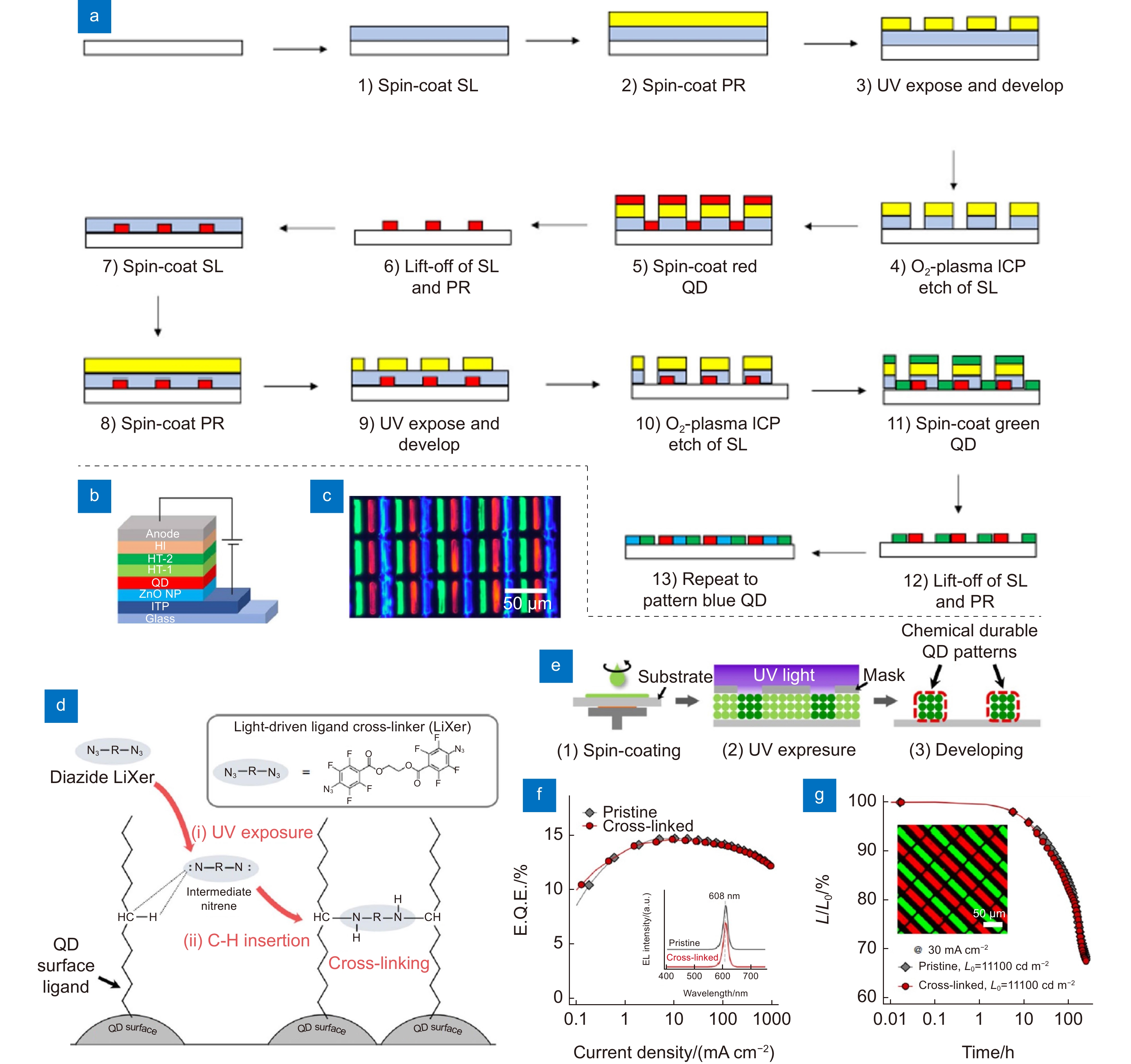
(a) Schematic illustration of patterning QDs with different color on a substrate via scarify layer assisted photolithography approach; (b) The device structure of Micro-QLED; (c) The electroluminescent image of the 500 ppi full-color Micro-QLED array[37]; (d) Schematic description of the ligand crosslinking process between neighboring quantum dots based on the C-H insertion reaction of the nitrene moiety of LiXer; (e) Schematic description of the photo-patterning processes of quantum dots using LiXer; (f) External quantum efficiency (EQE) – current density characteristics of pristine and cross-linked QLED devices; (g) Lifetime measurement of pristine and cross-linked QLED devices with an initial luminance of 11000 cd/m2. The sub pixel size in the inset image is 10 μm×38 μm[42]
-
Figure 13.
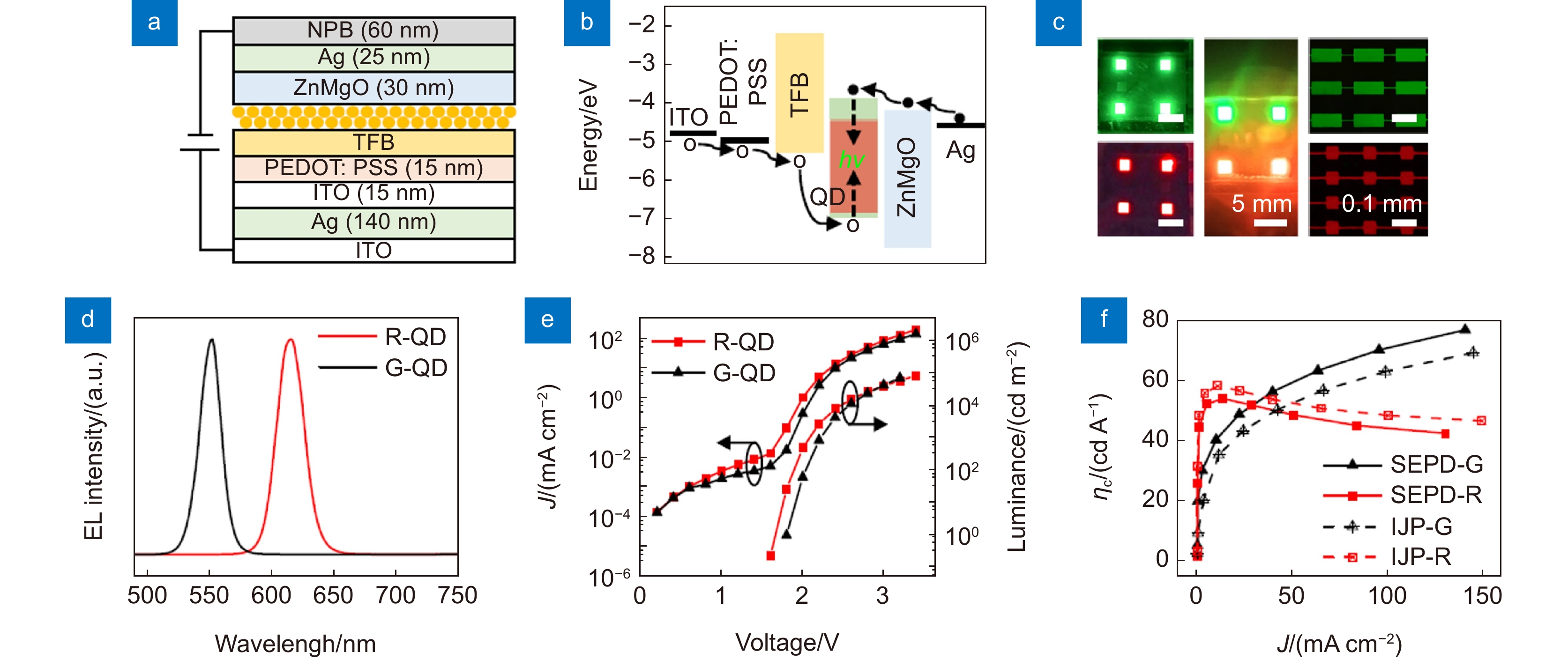
Optoelectronics properties of QLED by selective electrophoretic deposition.(a) Schematic diagram of the device structure of SEPD processed QLEDs; (b) Energy band diagram of the QLEDs; (c) Image of red and green SEPD QLED pixels. Scale bar: 5 mm and 0.1 mm; (d) Normalized electroluminescent spectra of red and green SEPD QLEDs; (e) Current density - luminance - voltage (J-L-V) characteristics of the red and green SEPD QLEDs; (f) Current efficiency - current density of SEPD QLED (solid line)[43]
-
Figure 14.
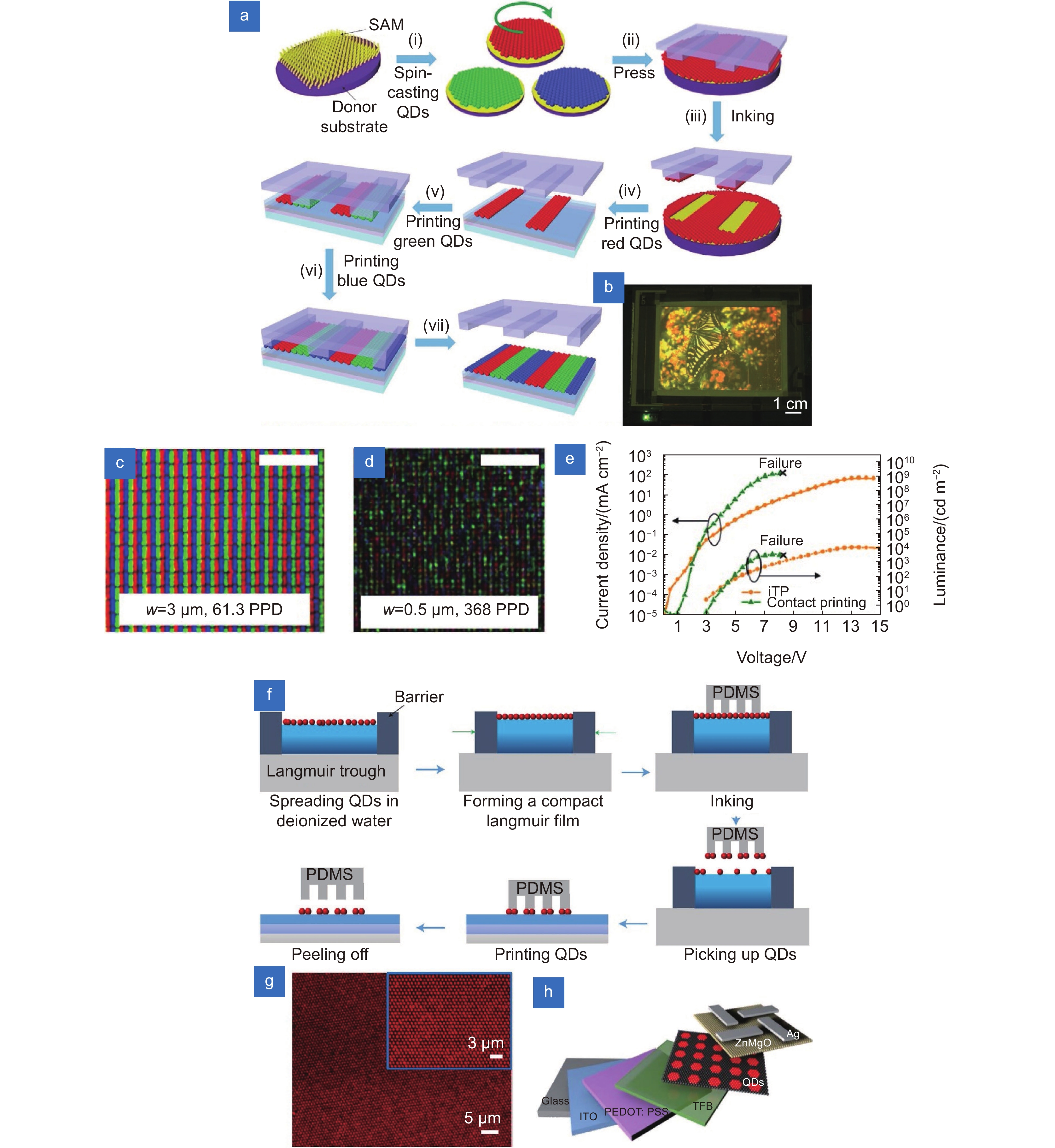
Micro-QLED by transfer printing.(a) Schematic of transfer printing process for patterning of quantum dots; (b) Electroluminescence image of a 4-inch full-color quantum dot display with a resolution of 320×240[60]; Confocal fluorescence images of full-color RGB quantum dots arrays with subpixel width of (c) 3 μm and (d) 0.5 μm; (e) Current density–voltage–luminance (J–V–L) characteristics of immersion transfer printing (yellow line) and contact printing (green line) devices[61]; (f) Schematic of the langmuir-Blodgett method assisted transfer printing process; (g) Fluorescence microscopy image of patterned red-QD-film arrays with scale bar of 5 μm and 3 μm (insert picture); (h) Schematic of the patterned red micro-QLED [62]
-
Figure 15.
Realization of full color Micro-QLED by optical resonant cavity[66]. (a) Schematic device structure of QLED; (b) Working principle of RGB micro-cavity based QLED; (c) The color coordinates and color triangle of the converted red, green, and blue emission. The color gamut can achieve 110% NTSC; (d) Pixelated QLED arrays with square pixel shape and subpixel size from 10 µm to 5 µm, and line shape with subpixel size from 3 µm to 1 µm
-
Figure 16.
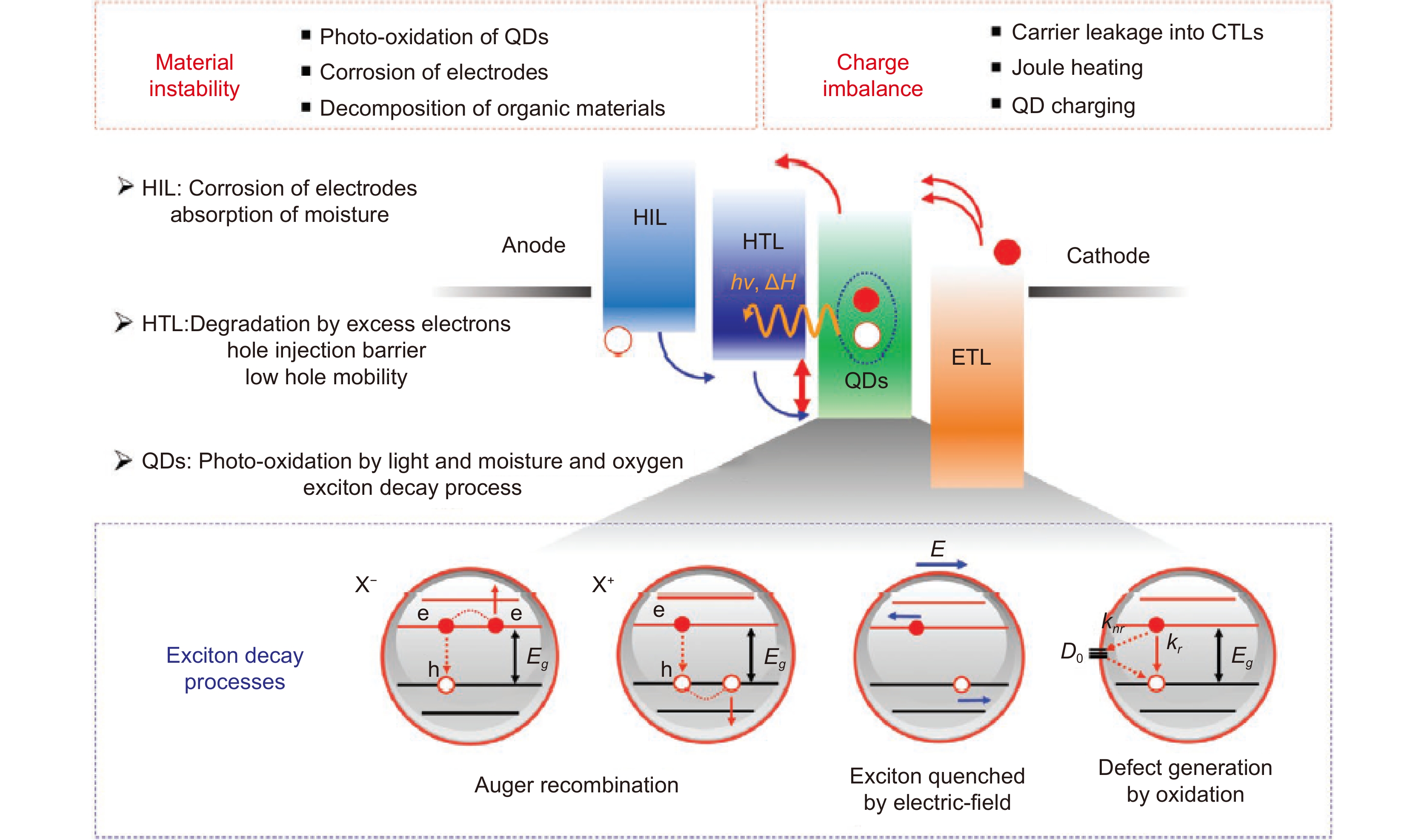
Degradation mechanism in QLEDs, including material instability, charge imbalance and exciton decay[54]
- Figure .


