2020 Vol. 3, No. 9
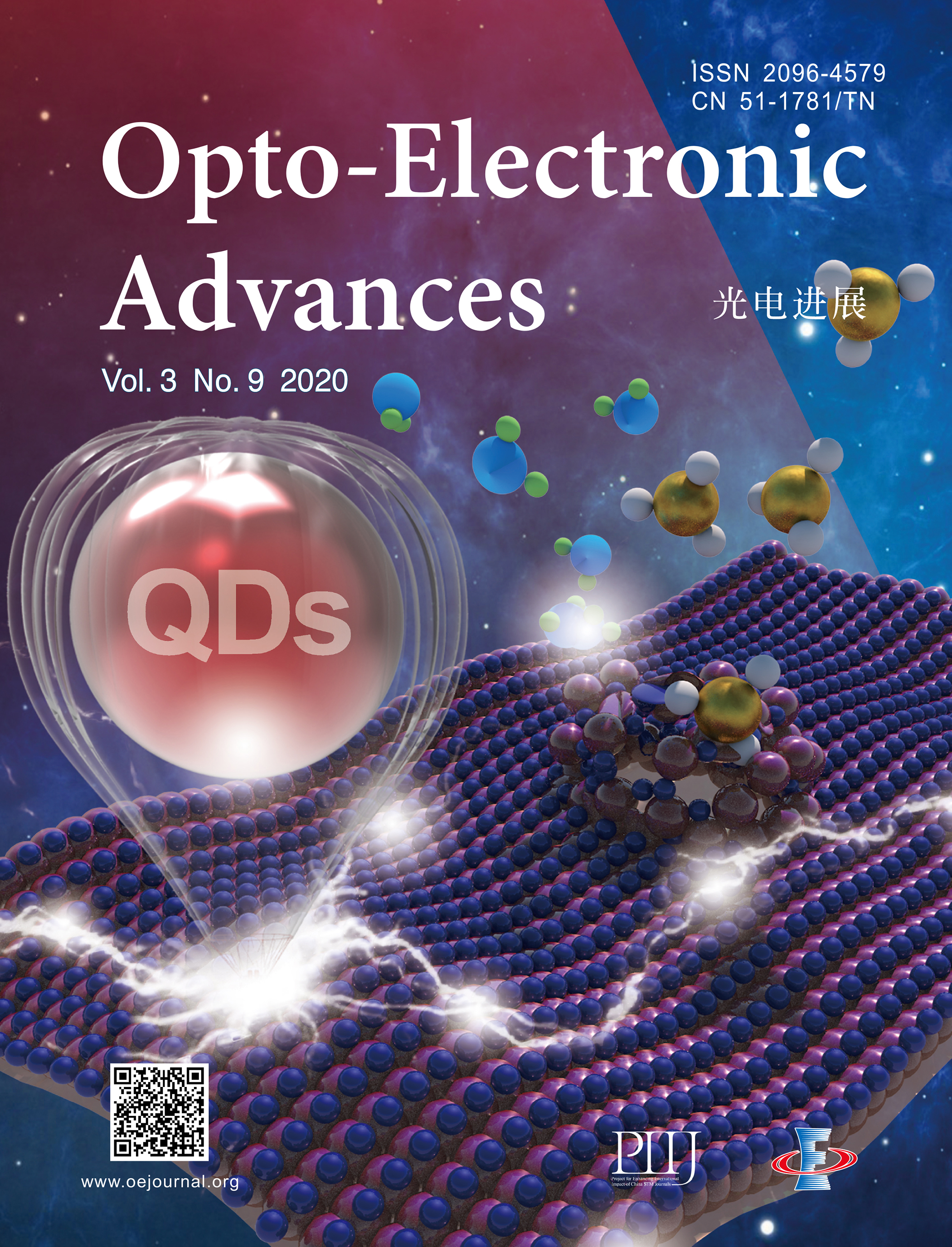
Cover Story: Zhou B Z, Liu M J, Wen Y W, Li Y, Chen R. Atomic layer deposition for quantum dots based devices. Opto-Electron Adv 3, 190043 (2020).
Quantum dots (QDs) are typical semiconductor nanocrystals with tunable band gaps, excellent photoluminescence efficiency and high extinction coefficient. And they are widely used in photodetectors, solar cells, light-emitting diodes (LED) and field effect transistors (FET). However, the photoluminescent quantum yield (PLQY) of QDs is severely limited by dangling bonds and trap states on the surface. In addition, the large specific surface area and exposed atomic sites are susceptible to the water/oxygen/light/heat in the environment. At the device level, the interface non-radiative recombination loss seriously affects the photoelectric performance of the QDs-based device. As a cross-scale fabrication technique, atomic layer deposition (ALD) meets the requirements of QD device fabrication and has been used in the modification of QDs and QDs-based devices. Recently, Professor Rong Chen in the micro-nano materials design and manufacturing research center at the College of Mechanical Science and Engineering of Huazhong University of Science and Technology reviewed ALD applications for QDs-based devices. ALD is suitable for surface defects passivation, dense thin film encapsulation, interstitial infilling and interface functional layers fabrication due to the characteristics of energy-dependent self-limiting reactions, dense uniform thin film fabrication, gas-phase infiltration and atomic level thickness control. This review has pointed out the direction of ALD for the development of new QDs-based devices in the future.

-
{{article.year}}, {{article.volume}}({{article.issue}}): {{article.fpage | processPage:article.lpage:6}}. doi: {{article.doi}}{{article.articleStateNameEn}}, Published online {{article.preferredDate | date:'dd MMMM yyyy'}}, doi: {{article.doi}}{{article.articleStateNameEn}}, Accepted Date {{article.acceptedDate | date:'dd MMMM yyyy'}}CSTR: {{article.cstr}}

 E-mail Alert
 RSS
RSS


