
 E-mail Alert
 RSS
RSS2022 Vol. 5, No. 5
Cover story: Li PH, Chen YJ, Wang BY, Li MM, Xiang D et al. Single-molecule optoelectronic devices: physical mechanism and beyond. Opto-Electron Adv 5, 210094 (2022)
Single-molecule electronic devices that use single molecules or molecular monolayers as their conductive channels provide a new strategy for solving the miniaturization and functionalization bottlenecks encountered by traditional semiconductor electronic devices. These devices have many inherent advantages, including miniaturization, adjustable electronic characteristics, functional diversity and so on. To date, single-molecule devices with a variety of functions have been realized, including diodes, field-effect devices and optoelectronic devices. In addition to their important applications in the field of functional devices, single-molecule devices also provide a unique platform to explore the intrinsic properties of matters at the single-molecule level. Controlling the electrical properties of single-molecule devices is still a key step to further advance the development of molecular electronics. The interaction between charge transport through single molecules and external fields, especially light, is very important and can be clarified by single-molecule optoelectronic devices. In this Review, Professor Xuefeng Guo and his co-authors introduce the optoelectronic effects involved in single-molecule devices, including photoisomerization switching, photoconductance, plasmon-induced excitation, photovoltaic effect and electroluminescence. In addition, they also summarize the optoelectronic mechanisms of single-molecule devices, with special emphasis on photoisomerization, photoexcitation and photo-assisted tunneling processes.

Back cover story: Li YX, Qian JM, Feng SJ, Chen Q, Zuo C. Deep-learning-enabled dual-frequency composite fringe projection profilometry for single-shot absolute 3D shape measurement. Opto-Electron Adv 5, 210021 (2022)
Fringe projection profilometry (FPP) has established itself as an essential optical three-dimensional (3D) imaging and measurement technique where the information about the 3D shape of an object to be measured is stored in the phase of a fringe pattern. Recovering the high-resolution absolute phase distribution from one single frame pattern has been the ultimate goal of FPP in perpetual pursuit. Frequency multiplexing, a long-established technique of sharing spectrum in telecommunications, has been introduced to FPP to encode two fringe patterns with different spatial carriers into a single snapshot measurement. However, it achieved limited success for measuring complex surfaces due to the unavoidable frequency overlapping and spectrum leakage. Recently, the research group of Prof. Chao Zuo at the Smart Computational Imaging Laboratory (SCILab) of Nanjing University of Science and Technology (NJUST) reported a deep-learning-enabled dual-frequency-multiplexing FPP technique. Through "learning" from a large number of data sets, a properly trained neural network can "de-multiplex" high-resolution, spectrally crosstalk-free phases from the composite fringe and directly reconstruct a high-accuracy absolute phase map for single-shot, unambiguous 3D surface imaging. This research opens new avenues for single-shot, instantaneous 3D shape measurement of discontinuous and/or mutually isolated objects in fast motion.
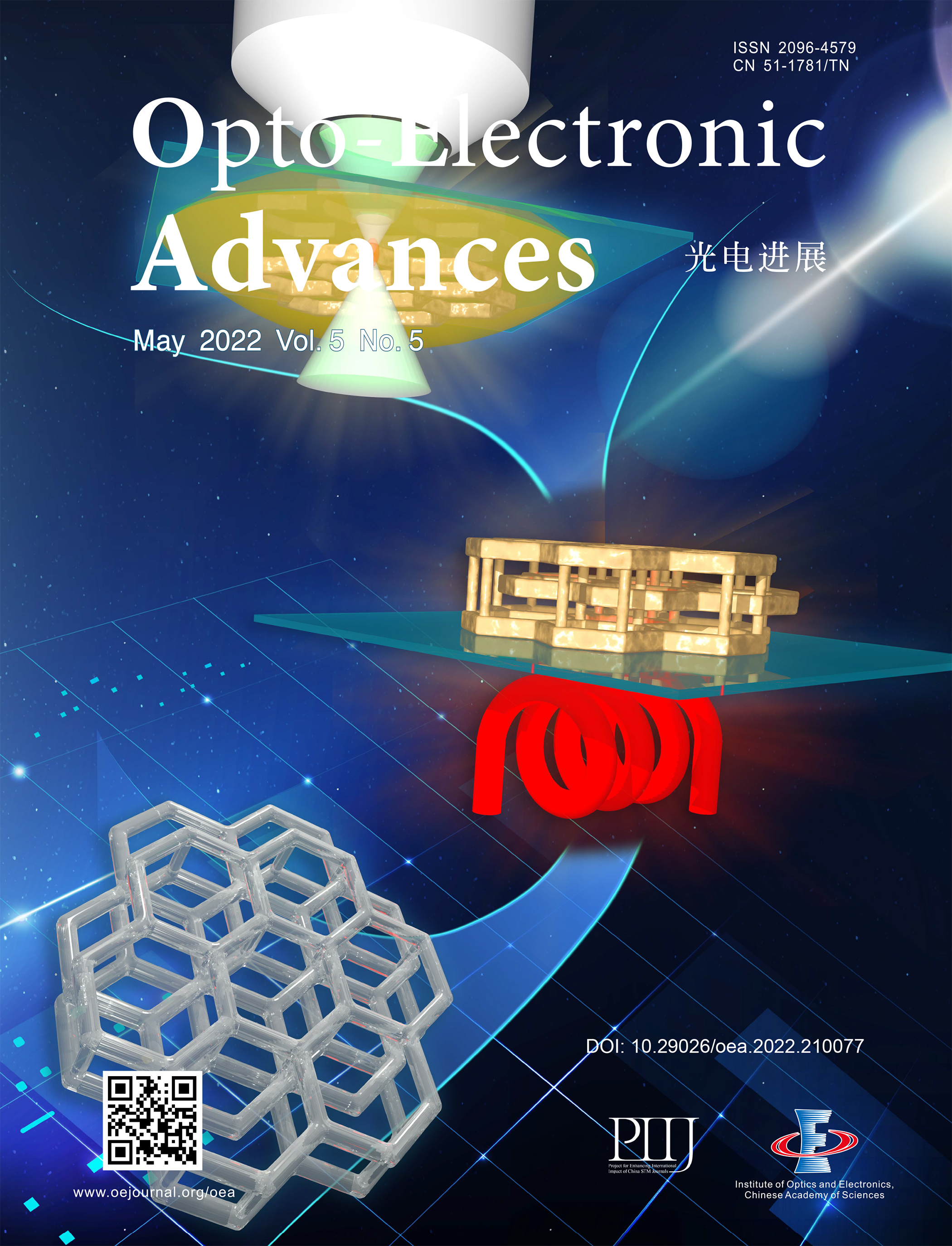
Inner cover story: Merkininkaitė G, Aleksandravičius E, Malinauskas M, Gailevičius D, Šakirzanovas S. Laser additive manufacturing of Si/ZrO2 tunable crystalline phase 3D nanostructures. Opto-Electron Adv 5, 210077 (2022).
A novel route for laser nano-printing of 3D crystalline structures was developed. The method employs ultrafast laser lithography, used as additive manufacturing tool for producing true 3D nanostructures, and combined with high temperature thermal post-treatment, converting the printed material into fully inorganic substance. The carried out inter-disciplinary experimental work was performed by Vilnius University scientists – an informal group of applied chemists and laser physicists united for mutual goal. Dr. Darius Gailevičius, Prof. Simas Šakirzanovas and Prof. Mangirdas Malinauskas revealed the potential of tuning the sintered ceramic structure into distinct crystalline phases, such as: cristobalite, SiO2, ZrSiO4, m-ZrO2, t-ZrO2. The proposed approach enabled achieving below 60 nm individual 3D features dimensions without any beam shaping or complex exposure techniques, thus makes it reproducible with other established standard or custom made laser direct writing setups. The principle is compatible with commercially available platforms (for instance: Nanoscribe, MultiPhoton Optics, Femtika, Workshop of Photonics, UpNano, MicroLight, and others). In brief, the validation of the combined laser manufacturing and thermal-treatment technique upgrades the widespread laser multi-photon lithography (also known as two-photon polymerization, two-photon lithography, laser direct writing lithography or simply optical micro-/nano-scale 3D printing) to a powerful tool enabling additive manufacturing of crystalline ceramics at unprecedented precision and three-dimensional flexibility. The achieved breakthrough is a milestone significantly contributing towards advancing the field of future opto-electronics.

-
{{article.year}}, {{article.volume}}({{article.issue}}): {{article.fpage | processPage:article.lpage:6}}. doi: {{article.doi}}{{article.articleStateNameEn}}, Published online {{article.preferredDate | date:'dd MMMM yyyy'}}, doi: {{article.doi}}{{article.articleStateNameEn}}, Accepted Date {{article.acceptedDate | date:'dd MMMM yyyy'}}CSTR: {{article.cstr}}
Prof. Xiangang Luo


