
 E-mail Alert
 RSS
RSS
| Citation: |

|
Polarized cavity ring-down technique for characterization of single-layer SiO2 films
-
Abstract
In this paper, a highly sensitive detection method - polarized cavity ring-down (P-CRD) technique - is employed to investigate the influence of deposition angle on the optical loss and stress-induced birefringence of single-layer SiO2 films prepared with specific deposition process parameters. The P-CRD technique is based on measuring the decay behavior of accumulated polarized light reflecting back and forth inside a resonant cavity. The decay time and oscillating frequency of resulted phase difference of the CRD signal are applied to measure simultaneously the absolute values of the optical loss and residual stress-induced birefringence at the same measurement point of single-layer SiO2 films. In the experiment, the optical losses and stress-induced birefringence of the single-layer SiO2 film samples prepared under different deposition angles of 60°, 70°, and 80° are measured and analyzed. The results revealed the effects of the changes of surface roughness and film compact density caused by the different deposition angles on the optical loss and stress-induced birefringence of the single-layer SiO2 films, respectively. These results are helpful to the preparation of high-performance SiO2 films with low optical loss and low residual stress.-
Keywords:
- polarized cavity ring-down /
- optical loss /
- stress induced birefringence /
- SiO2 films
-

-
References
[1] 范正修. 光学薄膜的损耗[J]. 中国激光, 1981, 8(8): 45–53 Fang Z X. Losses of optical thin films[J]. Chin J Lasers, 1981, 8(8): 45–53 [2] 荆建行, 孔明东, 王强, 等. 基于红外热像仪的光学薄膜吸收测试方法[J]. 光电工程, 2021, 48(6): 210071 doi: 10. 12086/oee 2021.210071 Jing J H, Kong M D, Wang Q, et al. Measurement of absorption loss of optical thin-film by infrared thermal imaging[J]. Opto-Electron Eng, 2021, 48(6): 210071 doi: 10. 12086/oee 2021.210071 [3] Dahmani F, Schmid A W, Lambropoulos J C, et al. Dependence of birefringence and residual stress near laser-induced cracks in fused silica on laser fluence and on laser-pulse number[J]. Appl Opt, 1998, 37(33): 7772–7784. doi: 10.1364/AO.37.007772 [4] 邵淑英, 范正修, 范瑞瑛, 等. ZrO2薄膜残余应力实验研究[J]. 光学学报, 2004, 24(4): 437–441 doi: 10.3321/j.issn:0253-2239.2004.04.002 Shao S Y, Fan Z X, Fan R Y, et al. Study of residual stress in ZrO2 thin films[J]. Acta Opt Sin, 2004, 24(4): 437–441 doi: 10.3321/j.issn:0253-2239.2004.04.002 [5] 邵淑英, 范正修, 范瑞瑛, 等. 薄膜应力研究[J]. 激光与光电子学进展, 2005, 42(1): 22–27 Shao S Y, Fan Z X, Fan R Y, et al. A review of study of stress in thin films[J]. Laser Optoelectron Prog, 2005, 42(1): 22–27 [6] Stout J H, Shores D A, Goedjen J G, et al. Stresses and cracking of oxide scales[J]. Mater Sci Eng A, 1989, 120–121: 193–197. [7] Sethuraman V A, Chon M J, Shimshak M, et al. In situ measurements of stress evolution in silicon thin films during electrochemical lithiation and delithiation[J]. J Power Sources, 2010, 195(15): 5062–5066. doi: 10.1016/j.jpowsour.2010.02.013 [8] 肖石磊, 李斌成. 光学元件残余应力无损检测技术概述[J]. 光电工程, 2020, 47(8): 190068 doi: 10.12086/oee.2020.190068 Xiao S L, Li B C. Residual stress measurement methods of optics[J]. Opto-Electron Eng, 2020, 47(8): 190068 doi: 10.12086/oee.2020.190068 [9] Xiao S L, Li B C, Cui H, et al. Sensitive measurement of stress birefringence of fused silica substrates with cavity ring-down technique[J]. Opt Lett, 2018, 43(4): 843–846. doi: 10.1364/OL.43.000843 [10] Huang H F, Lehmann K K. Effects of linear birefringence and polarization-dependent loss of supermirrors in cavity ring-down spectroscopy[J]. Appl Opt, 2008, 47(21): 3817–3827. doi: 10.1364/AO.47.003817 [11] Dupré P. Birefringence-induced frequency beating in high-finesse cavities by continuous-wave cavity ring-down spectroscopy[J]. Phys Rev A, 2015, 92(5): 053817. doi: 10.1103/PhysRevA.92.053817 [12] Fleisher A J, Long D A, Liu Q N, et al. Precision interferometric measurements of mirror birefringence in high-finesse optical resonators[J]. Phys Rev A, 2016, 93(1): 013833. doi: 10.1103/PhysRevA.93.013833 [13] Visschers J C, Tretiak O, Budker D, et al. continuous-wave cavity ring-down polarimetry[J]. J Chem Phys, 2020, 152(16): 164202. doi: 10.1063/5.0004476 [14] Atanassova E, Dimitrova T, Koprinarova J. AES and XPS study of thin RF-sputtered Ta2O5 layers[J]. Appl Surf Sci, 1995, 84(2): 193–202. doi: 10.1016/0169-4332(94)00538-9 [15] Neaton J B, Muller D A, Ashcroft N W. Electronic properties of the Si/SiO2 interface from first principles[J]. Phys Rev Lett, 2000, 85(6): 1298–1301. doi: 10.1103/PhysRevLett.85.1298 [16] Tomozeiu N. SiOx thin films deposited by r. f. magnetron reactive sputtering: structural properties designed by deposition conditions[J]. J Optoelectron Adv Mater, 2006, 8(2): 769–775. [17] 孔明东, 李斌成, 郭春, 等. SiO2光学薄膜的吸收边特性[J]. 光电工程, 2019, 46(4): 180220 doi: 10.12086/oee.2019.180220 Kong M D, Li B C, Guo C, et al. Characterictics of absorption edge of SiO2 films[J]. Opto-Electron Eng, 2019, 46(4): 180220 doi: 10.12086/oee.2019.180220 [18] Zheng M J, Zhang L D, Liu F M. Preparation and optical properties of SiO2 thin films containing InP nanocrystals[J]. Mater Res Bull, 2000, 35(14–15): 2469–2477. [19] Shintani A, Sugaki S, Nakashima H. Temperature dependence of stresses in chemical vapor deposited vitreous films[J]. J Appl Phys, 1980, 51(8): 4197–4205. doi: 10.1063/1.328277 [20] Revesz A G, Hughes H L. The structural aspects of non-crystalline SiO2 films on silicon: a review[J]. J Non Cryst Solids, 2003, 328(1–3): 48–63. [21] 林大伟, 黄伟, 熊胜明, 等. 不同沉积角度对氟化镱薄膜性质的影响[J]. 光电工程, 2011, 38(1): 103–106 doi: 10.3969j.issn.1003-501X.2011.01.020 Lin D W, Huang W, Xiong S M, et al. Effect of different deposition angle on the performance of YbF3 film[J]. Opto-Electron Eng, 2011, 38(1): 103–106 doi: 10.3969j.issn.1003-501X.2011.01.020 [22] Kupfer H, Flügel T, Richter F, et al. Intrinsic stress in dielectric thin films for micromechanical components[J]. Surf Coat Technol, 1999, 116–119: 116–120. [23] Choi J K, Lee J, Yoo J B, et al. Residual stress analysis of SiO2 films deposited by plasma-enhanced chemical vapor deposition[J]. Surf Coat Technol, 2000, 131(1–3): 153–157. [24] 王永珍, 龚国权, 崔敬忠. 二氧化硅薄膜的制备及应用[J]. 真空与低温, 2003, 9(4): 228–233 doi: 10.3969/j.issn.1006-7086.2003.04.010 Wang Y Z, Gong G Q, Cui J Z. Preparation and application of SiO2 thin films[J]. Vacuum Cryog, 2003, 9(4): 228–233 doi: 10.3969/j.issn.1006-7086.2003.04.010 [25] Wang B L, Oakberg T C. A new instrument for measuring both the magnitude and angle of low level linear birefringence[J]. Rev Sci Instrum, 1999, 70(10): 3847–3854. doi: 10.1063/1.1150000 [26] Fang M, Hu D F, Shao J D. Evolution of stress in evaporated silicon dioxide thin films[J]. Chin Opt Lett, 2010, 8(1): 119–122. doi: 10.3788/COL20100801.0119 [27] 张云洞, 刘洪祥. 离子束溅射沉积干涉光学薄膜技术[J]. 光电工程, 2001, 28(5): 69–72 doi: 10.3969/j.issn.1003-501X.2001.05.019 Zhang Y D, Liu H X. Production of optical coatings with ion beam sputter deposition technique[J]. Opto-Electron Eng, 2001, 28(5): 69–72 doi: 10.3969/j.issn.1003-501X.2001.05.019 [28] Amra C, Roche P, Pelletier E. Interface roughness cross-correlation laws deduced from scattering diagram measurements on optical multilayers: effect of the material grain size[J]. J Opt Soc Am B, 1987, 4(7): 1087–1093. doi: 10.1364/JOSAB.4.001087 [29] 侯海虹, 孙喜莲, 申雁鸣, 等. 电子束蒸发氧化锆薄膜的粗糙度和光散射特性[J]. 物理学报, 2006, 55(6): 3124–3127 doi: 10.3321/j.issn:1000-3290.2006.06.081 Hou H H, Sun X L, Shen Y M, et al. Roughness and light scattering properties of ZrO2 thin films deposited by electron beam evaporation[J]. Acta Phys Sin, 2006, 55(6): 3124–3127 doi: 10.3321/j.issn:1000-3290.2006.06.081 [30] 侯海虹, 孙喜莲, 田光磊, 等. 利用总积分散射仪对光学薄膜表面散射特性的研究[J]. 物理学报, 2009, 58(9): 6425–6429 doi: 10.3321/j.issn:1000-3290.2009.09.088 Hou H H, Sun X L, Tian G L, et al. Research on the surface scattering properties of optical films by the total integrated scatter[J]. Acta Phys Sin, 2009, 58(9): 6425–6429 doi: 10.3321/j.issn:1000-3290.2009.09.088 [31] 顾培夫. 薄膜技术[M]. 杭州: 浙江大学出版社, 1990: 80–81 Gu P F. Technology of Thin Film[M]. Hangzhou: Zhejiang University Press, 1990: 80–81 -
Overview

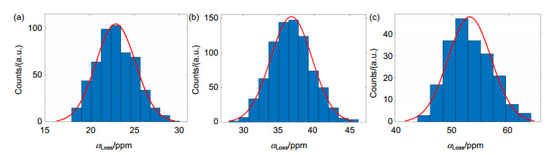
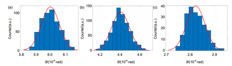
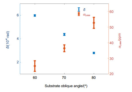
Overview: Silicon dioxide (SiO2) is a preferred low index of refraction material for preparing high-performance optical films because of its low absorption coefficient, high corrosion resistance, high hardness, and so on. During the preparation of optical thin films, the residual stress inside the films needs to be well controlled; otherwise, it may cause surface deformation and refractive index anisotropy of corresponding optical components. There are many methods for measuring residual stress inside optical components that have limited measurement accuracy, such as the Stoney curvature method, X-ray diffraction (XRD) method, photoelastic modulator (PEM) method, and so on. In this paper, the stress birefringence measurement method based on polarized cavity ring-down (P-CRD) is adopted to measure simultaneously the residual stress-induced birefringence and optical loss of single-layer SiO2 film samples. In P-CRD, the measurement of stress birefringence and optical loss is not affected by the fluctuation of light intensity as instead a delay time is measured. The measurement accuracy of the stress birefringence is significantly improved due to the cumulative effect of the polarization phase difference by multiple back and forth reflections inside the ring-down cavity. In order to explore the influence of deposition angle on the optical loss and stress birefringence of single-layer SiO2 film samples prepared with Ion-Beam Sputtering (IBS) coating technique, three single-layer SiO2 film samples with deposition angles of 60°, 70° and 80° were measured with P-CRD. The achieved measurement precisions were less than 3.5 ppm for the optical loss and 5.0×10⁻⁶ rad for the stress refringence. The measured optical losses were 22.9 ppm, 36.4 ppm, and 52.7 ppm, and the stress birefringence were 5.99×10⁻⁴ rad, 4.38×10⁻⁴ rad, and 2.80×10⁻⁴ rad for the samples prepared with deposition angles of 60°, 70°, and 80°, respectively. Clearly, as the deposition angle increases, the optical loss increases and the stress birefringence decreases.
The scattering losses of the single-layer SiO2 film samples were also measured with a Total Integrated Scattering (TIS) instrument. The scattering measurement results showed that as the deposition angle increases, the surface roughness of the single-layer SiO2 film gradually increases, resulting in increased surface scattering, which in turn increases the optical loss measured by P-CRD. In addition, the increase in surface roughness makes the film more prone to a loose and porous structure. Since the residual stress has a strong correlation with the packing density of the film, a loose structure indicates a reduced packing density, which causes the residual stress (and the stress-induced birefringence) of the film sample to decrease gradually with the increasing deposition angle.
These results not only confirmed that the polarization cavity ring-down technique has higher stress birefringence measurement accuracy than the currently most sensitive instrument based on PEM (with phase difference measurement accuracy of 5×10⁻⁵ rad), but also were helpful to the preparation of high-performance SiO2 films with low optical loss and low residual stress.
-
Access History
Figures(7)
Tables(3)
Article Metrics

Export File
Citation
Format
Content
 DownLoad:
-
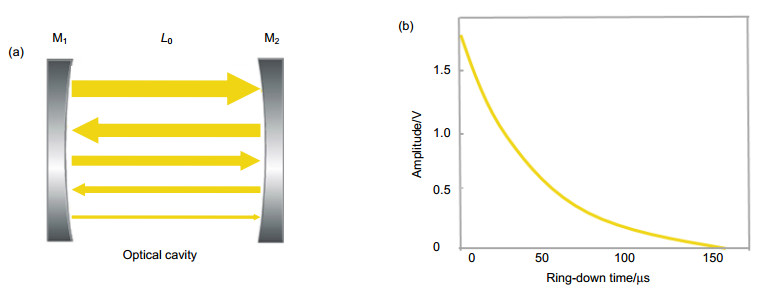
Figure 1.
The initial cavity configuration (a) and corresponding ring-down curve (b) for a cavity ring-down technique
-
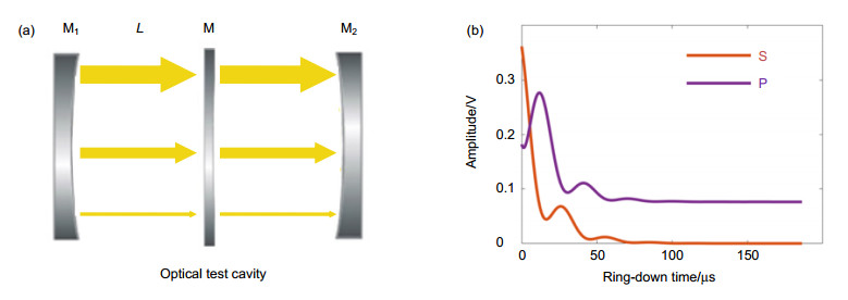
Figure 2.
Test cavity configuration (a) and the corresponding oscillation ring-down curve (b)
-
Figure 3.
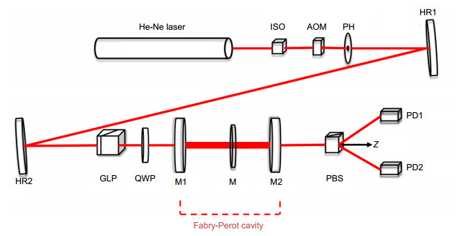
Experimental arrangement of polarized cavity ring-down to measure the optical loss and stress-induced birefringence of optical components.
-
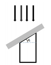
Figure 4.
Oblique deposition technique to prepare single-layer film samples
-
Figure 5.
Optical loss statistical distribution and corresponding Gaussian fitting of single-layer film samples prepared at different deposition angles. (a) 60°; (b) 70°; (c) 80°
-
Figure 6.
Statistical distribution of stress birefringence phase difference and corresponding Gaussian fitting of single-layer film samples prepared at different deposition angles. (a) 60°; (b) 70°; (c) 80°
-
Figure 7.
The influence of deposition angle on optical loss and residual stress of single-layer film samples


