
 E-mail Alert
 RSS
RSS
| Citation: |
Yang R, Yu Q Q, Pan Y W, et al. Directional-multiplexing holography by on-chip metasurface[J]. Opto-Electron Eng, 2022, 49(10): 220177. doi: 10.12086/oee.2022.220177

|
Directional-multiplexing holography by on-chip metasurface
-
Abstract
The on-chip metasurface is introduced into integrated optical waveguides to achieve arbitrary modulation of guided waves, which provides a convenient and versatile platform for the conversion between guided waves and free-space functions. Despite previous explorations in on-chip holography demonstration, it still faces critical challenges to expand the encoding freedom and multiplexing. Here, we propose and experimentally demonstrate a quad-fold multiplexed holographic display optics device based on an on-chip metasurface. By mixing the detour phase and Pancharatnam-Berry (PB) phase, the on-chip metasurface couples the guided waves into free space in circular polarization, destroying the phase degeneracy that exists in the wavevector directions with only the detour phase. Moreover, by utilizing simulated annealing phase optimization algorithm and multiplexing, we achieved a quad-fold multiplexed far-field holographic display with independent encoding capability. The proposed method in this paper opens up a new prospect for multifunctional integration of on-chip metasurfaces and provides an alternative approach for integrated optical communication with high information storage capacity. -

-
References
[1] 郭旭岳, 李冰洁, 樊鑫豪, 等. 基于电介质超表面的光场复振幅调制及应用[J]. 红外与激光工程, 2020, 49(9): 20201031. doi: 10.3788/IRLA20201031 Guo X Y, Li B J, Fan X H, et al. Complex amplitude modulation of light fields based on dielectric metasurfaces and its applications[J]. Infrared Laser Eng, 2020, 49(9): 20201031. doi: 10.3788/IRLA20201031 [2] 杨渤, 程化, 陈树琪, 等. 基于傅里叶分析的超表面多维光场调控[J]. 光学学报, 2019, 39(1): 0126005. doi: 10.3788/AOS201939.0126005 Yang B, Cheng H, Chen S Q, et al. Multi-dimensional manipulation of optical field by metasurfaces based on Fourier analysis[J]. Acta Opt Sin, 2019, 39(1): 0126005. doi: 10.3788/AOS201939.0126005 [3] 李雄, 马晓亮, 罗先刚. 超表面相位调控原理及应用[J]. 光电工程, 2017, 44(3): 255−275. doi: 10.3969/j.issn.1003-501X.2017.03.001 Li X, Ma X L, Luo X G. Principles and applications of metasurfaces with phase modulation[J]. Opto-Electron Eng, 2017, 44(3): 255−275. doi: 10.3969/j.issn.1003-501X.2017.03.001 [4] Wan S, Tang J, Wan C W, et al. Angular‐encrypted quad‐fold display of nanoprinting and meta‐holography for optical information storage[J]. Adv Opt Mater, 2022, 10(11): 2102820. doi: 10.1002/adom.202102820 [5] Tang J, Wan S, Shi Y Y, et al. Dynamic augmented reality display by layer‐folded metasurface via electrical‐driven liquid crystal[J]. Adv Opt Mater, 2022, 10(12): 2200418. doi: 10.1002/adom.202200418 [6] Cao T, Lian M, Liu K, et al. Wideband mid-infrared thermal emitter based on stacked nanocavity metasurfaces[J]. Int J Extreme Manuf, 2022, 4(1): 015402. doi: 10.1088/2631-7990/ac3bb1 [7] Wang Z J, Dai C J, Li Z, et al. Free-space optical merging via meta-grating inverse-design[J]. Nano Lett, 2022, 22(5): 2059−2064. doi: 10.1021/ACS.NANOLETT.1C05026 [8] Wan C W, Li Z, Wan S, et al. Electric‐driven meta‐optic dynamics for simultaneous near‐/far‐field multiplexing display[J]. Adv Funct Mater, 2022, 32(10): 2110592. doi: 10.1002/adfm.202110592 [9] Wang Z J, Dai C J, Zhang J, et al. Real‐time tunable nanoprinting‐multiplexing with simultaneous meta‐holography displays by stepwise nanocavities[J]. Adv Funct Mater, 2022, 32(9): 2110022. doi: 10.1002/adfm.202110022 [10] Zhang D S, Liu R J, Li Z G, et al. Irregular LIPSS produced on metals by single linearly polarized femtosecond laser[J]. Int J Extreme Manuf, 2022, 4(1): 015102. doi: 10.1088/2631-7990/ac376c [11] Li Z Y, Kim M H, Wang C, et al. Controlling propagation and coupling of waveguide modes using phase-gradient metasurfaces[J]. Nat Nanotechnol, 2017, 12(7): 675−683. doi: 10.1038/nnano.2017.50 [12] Meng Y, Liu Z T, Xie Z W, et al. Versatile on-chip light coupling and (de)multiplexing from arbitrary polarizations to controlled waveguide modes using an integrated dielectric metasurface[J]. Photonics Res, 2020, 8(4): 564−576. doi: 10.1364/PRJ.384449 [13] Ding F, Deshpande R, Bozhevolnyi S I. Bifunctional gap-plasmon metasurfaces for visible light: polarization-controlled unidirectional surface plasmon excitation and beam steering at normal incidence[J]. Light Sci Appl, 2018, 7: 17178. doi: 10.1038/lsa.2017.178 [14] Yang R, Shi Y Y, Wan S, et al. On-chip metasurface for optical directional rectification[J]. J Lightwave Technol, 2021, 39(17): 5558−5562. doi: 10.1109/JLT.2021.3091431 [15] Shi Y Y, Yang R, Dai C J, et al. On-chip asymmetric beam-steering for broadband visible light[J]. Opt Lett, 2022, 47(2): 369−372. doi: 10.1364/OL.443888 [16] Wang Z, Li T T, Soman A, et al. On-chip wavefront shaping with dielectric metasurface[J]. Nat Commun, 2019, 10(1): 3547. doi: 10.1038/s41467-019-11578-y [17] Yang R, Shi Y Y, Dai C J, et al. On-chip metalenses based on one-dimensional gradient trench in the broadband visible[J]. Opt Lett, 2020, 45(20): 5640−5643. doi: 10.1364/OL.405446 [18] Ding Y M, Chen X, Duan Y, et al. Metasurface-dressed two-dimensional on-chip waveguide for free-space light field manipulation[J]. ACS Photonics, 2022, 9(2): 398−404. doi: 10.1021/acsphotonics.1c01577 [19] Zhou N, Zheng S, Cao X P, et al. Ultra-compact broadband polarization diversity orbital angular momentum generator with 3.6 x 3.6 μm2 footprint[J]. Sci Adv, 2019, 5(5): eaau9593. doi: 10.1126/sciadv.aau9593 [20] Yang R, Wan S, Shi Y Y, et al. Immersive tuning the guided waves for multifunctional on‐chip metaoptics[J]. Laser Photonics Rev, 2022, 16(8): 2200127. doi: 10.1002/LPOR.202200127 [21] Shi Y Y, Wan C W, Dai C J, et al. Augmented reality enabled by on‐chip meta‐holography multiplexing[J]. Laser Photonics Rev, 2022, 16(6): 2100638. doi: 10.1002/lpor.202100638 [22] Shi Y Y, Wan C W, Dai C J, et al. On-chip meta-optics for semi-transparent screen display in sync with AR projection[J]. Optica, 2022, 9(6): 670−676. doi: 10.1364/OPTICA.456463 [23] Huang Z Q, Marks D L, Smith D R. Out-of-plane computer-generated multicolor waveguide holography[J]. Optica, 2019, 6(2): 119−124. doi: 10.1364/OPTICA.6.000119 [24] Gao H, Fan X H, Xiong W, et al. Recent advances in optical dynamic meta-holography[J]. Opto-Electron Adv, 2021, 4(11): 210030. doi: 10.29026/oea.2021.210030 [25] Yulaev A, Zhu W Q, Zhang C, et al. Metasurface-integrated photonic platform for versatile free-space beam projection with polarization control[J]. ACS Photonics, 2019, 6(11): 2902−2909. doi: 10.1021/acsphotonics.9b01000 [26] Guo X X, Ding Y M, Chen X, et al. Molding free-space light with guided wave–driven metasurfaces[J]. Sci Adv, 2020, 6(29): eabb4142. doi: 10.1126/sciadv.abb4142 [27] Fang B, Wang Z Z, Gao S L, et al. Manipulating guided wave radiation with integrated geometric metasurface[J]. Nanophotonics, 2022, 11(9): 1923−1930. doi: 10.1515/NANOPH-2021-0466 [28] Ha Y L, Guo Y H, Pu M B, et al. Monolithic‐integrated multiplexed devices based on metasurface‐driven guided waves[J]. Adv Theory Simul, 2021, 4(2): 2000239. doi: 10.1002/ADTS.202000239 [29] Lin J, Genevet P, Kats M A, et al. Nanostructured holograms for broadband manipulation of vector beams[J]. Nano Lett, 2013, 13(9): 4269−4274. doi: 10.1021/nl402039y [30] Pancharatnam S. Generalized theory of interference and its applications: Part II. Partially coherent pencils[J]. Proc Indiana Acad Sci, 1956, 44(6): 398−417. doi: 10.1007/BF03046095 [31] Zhan Q W, Leger J R. Interferometric measurement of the geometric phase in space-variant polarization manipulations[J]. Opt Commun, 2002, 213(4–6): 241−245. doi: 10.1016/S0030-4018(02)02123-5 [32] Chrostowski L, Hochberg M. Silicon Photonics Design: from Devices to Systems[M]. New York: Cambridge University Press, 2015. [33] Li L L, Cui T J, Ji W, et al. Electromagnetic reprogrammable coding-metasurface holograms[J]. Nat Commun, 2017, 8(1): 197. doi: 10.1038/s41467-017-00164-9 [34] Zheng G X, Mühlenbernd H, Kenney M, et al. Metasurface holograms reaching 80% efficiency[J]. Nat Nanotechnol, 2015, 10(4): 308−312. doi: 10.1038/nnano.2015.2 -
Overview
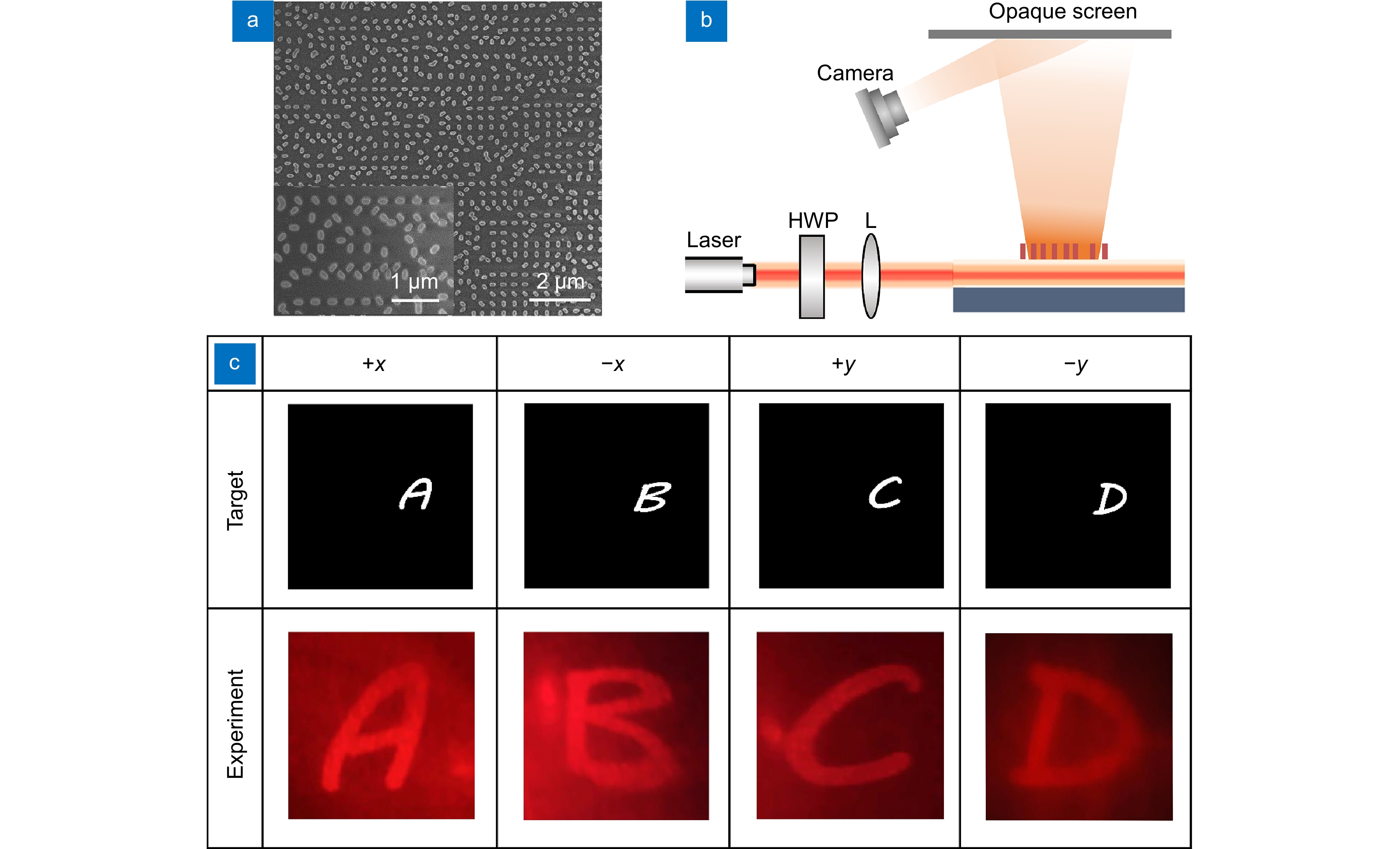
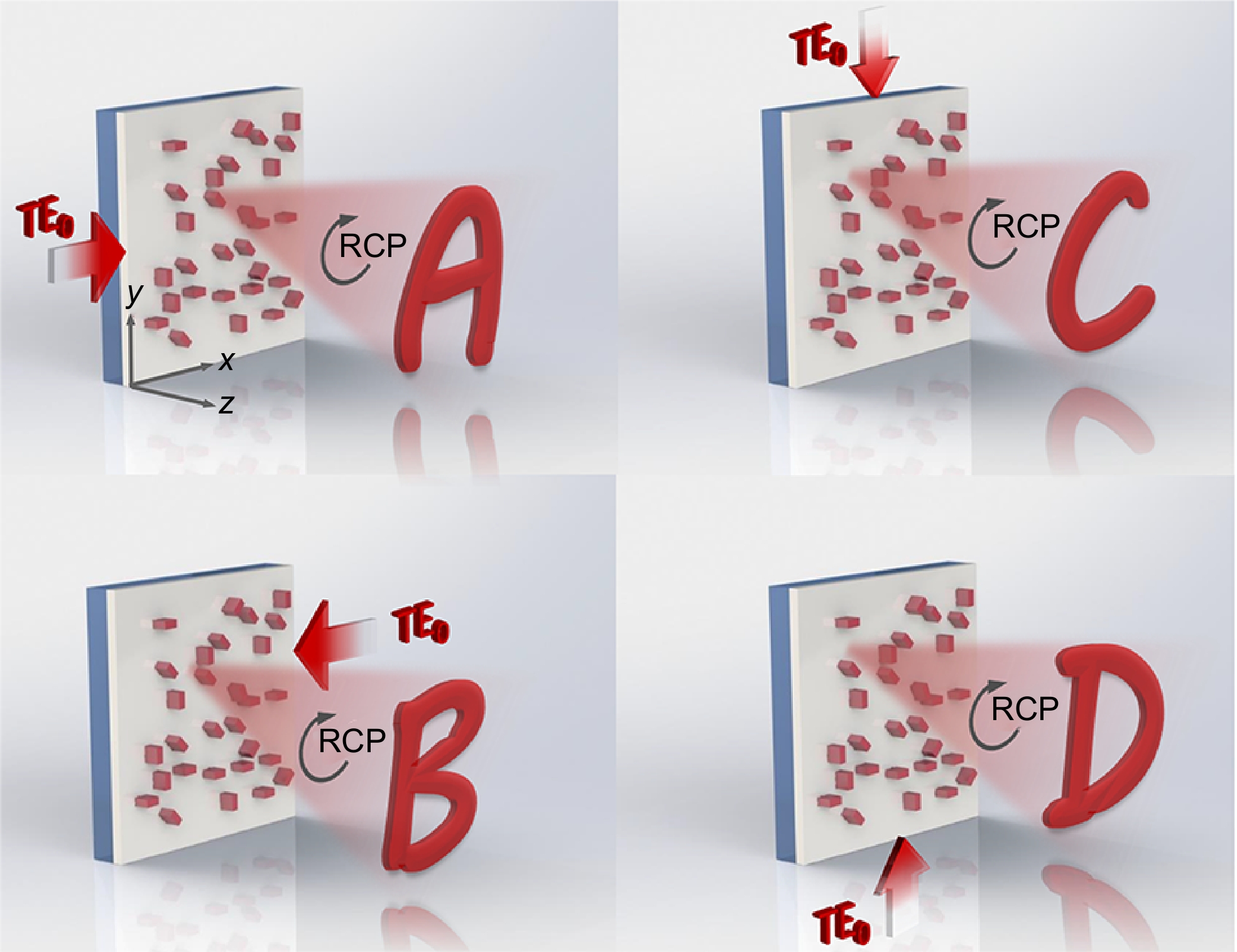
Photonic integrated circuits (PIC) serve as an essential and promising candidate to eventually replace electronic circuits for the next-generation information processing. However, traditional PIC devices based on optical waveguides are usually bulky and lack full control at the subwavelength scale to achieve arbitrary wavefront-shaping functionalities. Recently, the invention of on-chip metasurface promotes the connection between guided and free-space optics and realizes the arbitrary conversion of guided waves and free-space light. As a new type of on-chip nanophotonic device, the introduction of metasurface onto the optical waveguide has made significant progress and exhibited multi-functional conversion from the guided waves to free-space, including directional beam-steering emitters, mode-conversion, on-chip lensing, optical router, and on-chip holography, etc. These on-chip nanophotonics devices provide new avenues for photonic chip-scale devices and miniature on-chip systems. For instance, meta-holography is an emerging and universal strategy based on engineered nanoantennas array to construct an optical-field image. However, on-chip far-field holographs are limited for realizing multiplexing for multiple directions due to a lack the arbitrary-encoding capability because their detour phases are complementarily related when the source propagates and excites the on-chip array from either positive or negative direction. Here, we propose and experimentally demonstrate a quad-fold multiplexed far-filed holographic display optics device based on an on-chip metasurface. This optics device is composed of silicon nanopillar arrays on top of a planar waveguide of Si3N4, in which a relatively thick layer of silica serves as the bottom cladding substrate. By mixing the detour phase and Pancharatnam-Berry (PB) phase, the on-chip metasurface could couple the guided waves into free space in circular polarization. The phase degeneracy in the positive and negative directions could be decoupled by selecting the desired circular polarization. Subsequently, utilizing a simulated annealing phase optimization algorithm to optimize the phase required by holograms and the multiplexing technology of on-chip directional, we achieved a quad-fold multiplexed far-field holographic display with independent encoding capability. Eventually, to verify the on-chip quad-fold multiplexed holography performance, we fabricated an on-chip metasurface sample by the conventional electron-beam lithography technique and the reactive ion etching processing. Through end-fire coupling from the laser source at λ = 650 nm into the on-chip metasurface sample along ±x/±y - directions, the far-field holographic images of the four letters (“A”, “B”, “C”, and “D”) multiplexing are successfully observed at their corresponding areas. The method proposed here opens up new prospects for the multifunctional integration of on-chip metasurfaces and provides an alternative approach for integrated optical communication with high information storage capacity.
-
Access History

Export File
Citation
Yang R, Yu Q Q, Pan Y W, et al. Directional-multiplexing holography by on-chip metasurface[J]. Opto-Electron Eng, 2022, 49(10): 220177. doi: 10.12086/oee.2022.220177
Format
Content
 DownLoad:
-
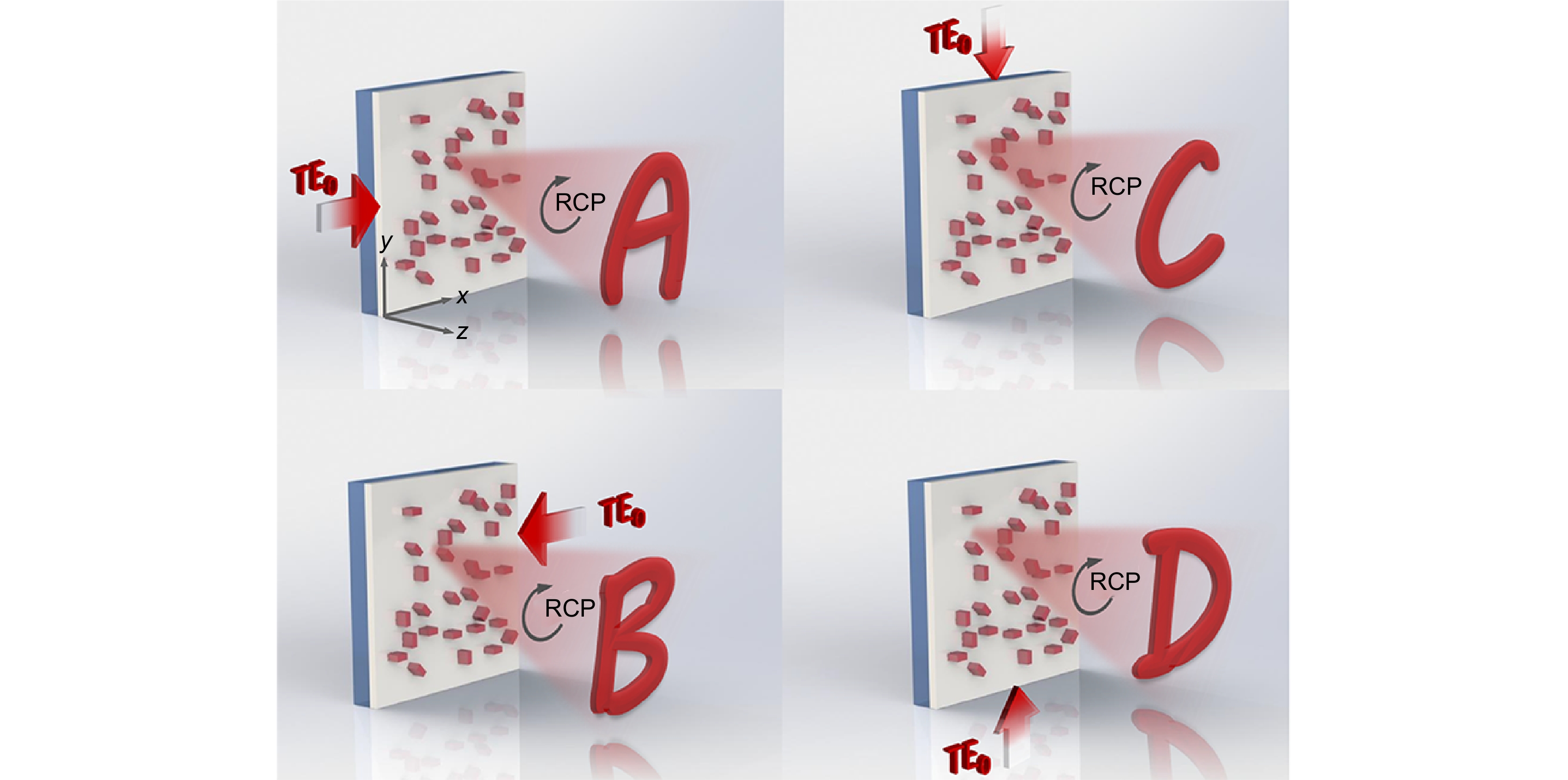
Figure 1.
Schematic diagram of the on-chip four-channel multiplexed holography. Four diverse holographic images (“A/B/C/D”) in the far-field could be displayed by the on-chip metasurface integrated on the waveguide, when the laser source is end-fire coupled into the waveguide along the ±x and ±y directions, respectively
-
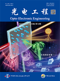
Figure 2.
On-chip metasurface mechanism for controlling the phase of extracted guided waves. (a) Schematic of the unit cell to compose the on-chip metasurface; (b) The principle of guided wave extraction by combining the detour phase and geometric phase; (c) The correspondence between discrete detour phases and the positions of meta-atoms in the unit cell; (d) The relationship between discrete geometric phase delay and the orientation angle of the meta-atoms
-
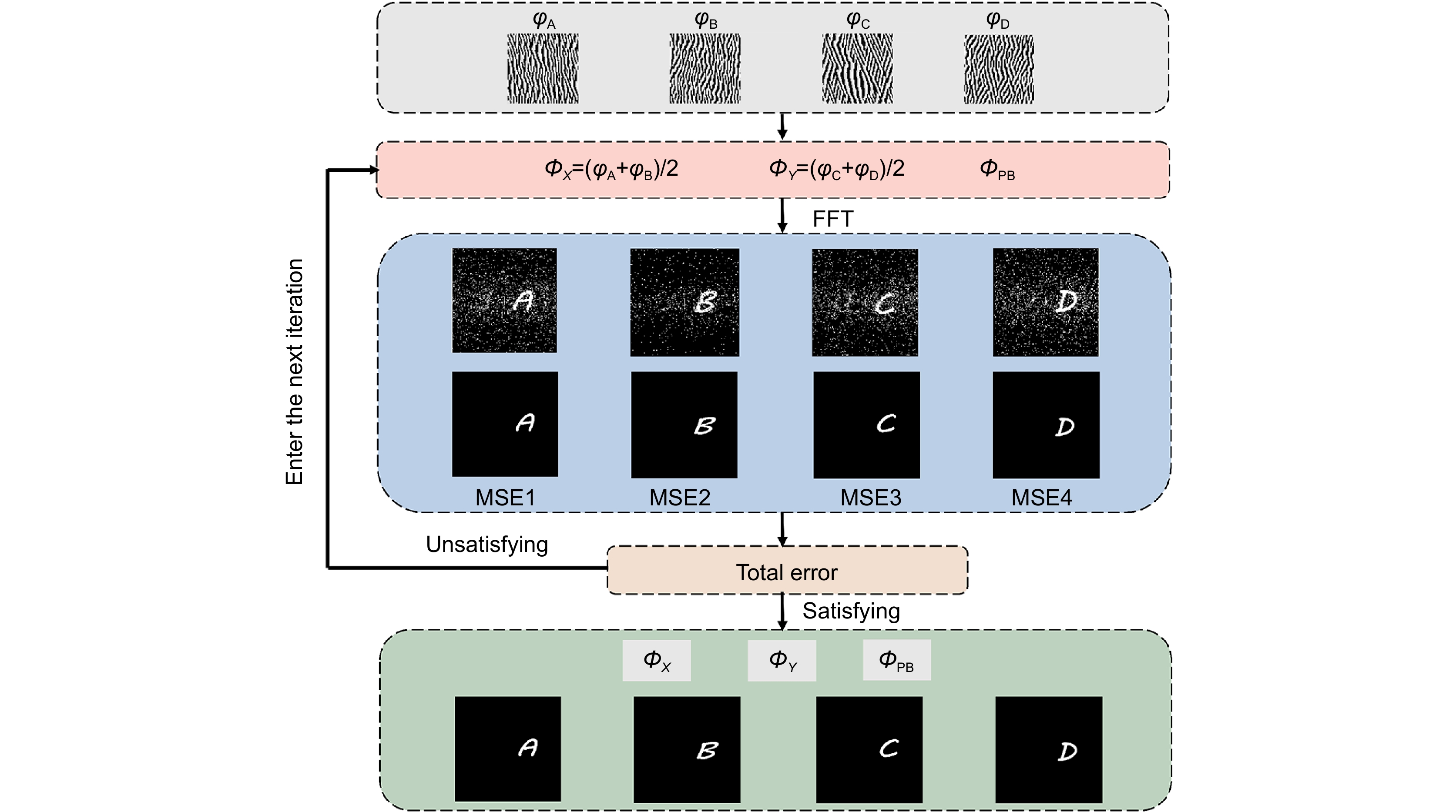
Figure 3.
Phase optimization flowchart for the on-chip quad-fold multiplexed holography
-
Figure 4.
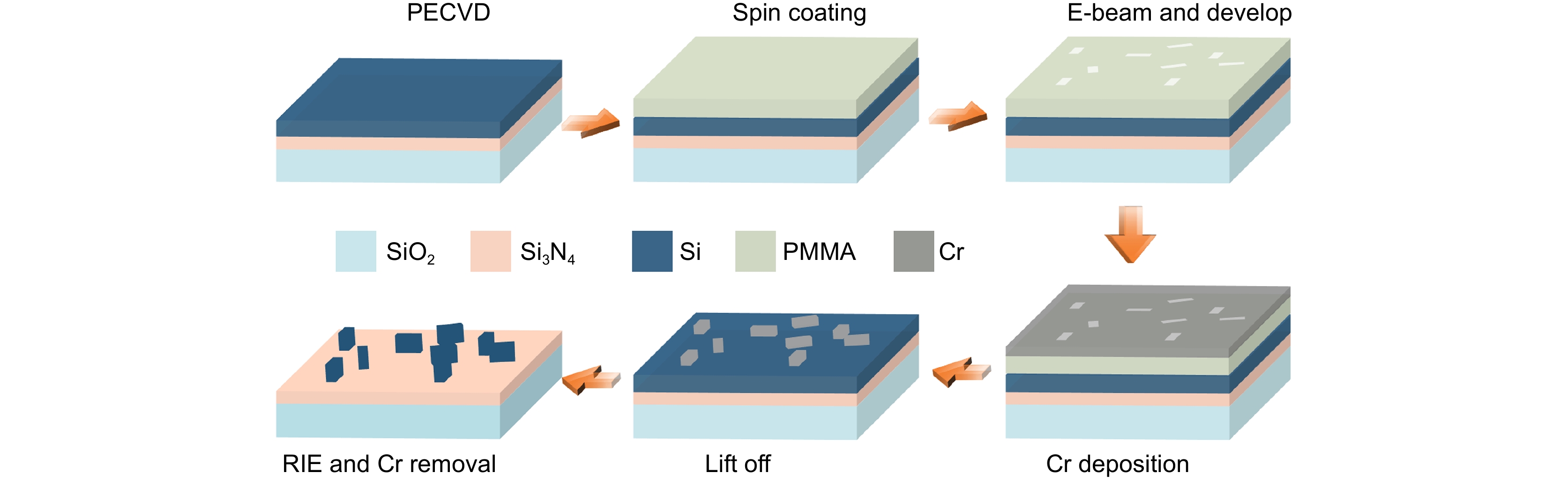
The sample fabrication flow chart of the on-chip quad-fold multiplexing holographic metasurface
-
Figure 5.
Experimental verification for the on-chip quad-fold holography. (a) The overall SEM image and zoom-in SEM image of the fabricated sample; (b) Optical experimental setup sketch for measuring on-chip quad-fold holography; (c) Target and experimental holograms measured in the area corresponding to the target for guided waves incidence from the ±x/±y direction, respectively
- Figure .


