
 E-mail Alert
 RSS
RSS
| Citation: |

|
Silicon cuboid nanoantenna with simultaneous large Purcell factor for electric dipole, magnetic dipole and electric quadrupole emission
-
Abstract
The Purcell effect is commonly used to increase the spontaneous emission rate by modifying the local environment of a light emitter. Here, we propose a silicon dielectric cuboid nanoantenna for simultaneously enhancing electric dipole (ED), magnetic dipole (MD) and electric quadrupole (EQ) emission. We study the scattering cross section, polarization charge distribution, and electromagnetic field distribution for electromagnetic plane wave illuminating the silicon dielectric cuboid nanoantenna, from which we have identified simultaneous existence of ED, MD and EQ resonance modes in this nanoantenna. We have calculated the Purcell factor of ED, MD and EQ emitters with different moment orientations as a function of radiation wavelength by placing these point radiation source within the nanoantenna, respectively. We find that the resonances wavelengths of the Purcell factor spectrum are matching with the resonance modes in the nanoantenna. Moreover, the maximum Purcell factor of these ED, MD and EQ emitters is 18, 150 and 118 respectively, occurring at the resonance wavelength of 475, 750, and 562 nm, respectively, all within the visible range. The polarization charge distribution features allow us to clarify the excitation and radiation of these resonance modes as the physical origin of large Purcell factor simultaneously occurring in this silicon cuboid nanoantenna. Our theoretical results might help to deeply explore and design the dielectric nanoantenna as an ideal candidate to enhance ED, MD and EQ emission simultaneously with very small loss in the visible range, which is superior than the more popular scheme of plasmonic nanoantenna.-
Keywords:
- dielectric nanostructure /
- spontaneous emission /
- resonance /
- Purcell effect
-

-
References
[1] Kinkhabwala A, Yu ZF, Fan SH, Avlasevich Y, Müllen K et al. Large single-molecule fluorescence enhancements produced by a bowtie nanoantenna. Nat Photonics 3, 654–657 (2009). doi: 10.1038/nphoton.2009.187 [2] Noginov MA, Zhu G, Belgrave AM, Bakker R, Shalaev VM et al. Demonstration of a spaser-based nanolaser. Nature 460, 1110–1114 (2009). doi: 10.1038/nature08318 [3] Oulton RF, Sorger VJ, Zentgraf T, Ma RM, Gladden C et al. Plasmon lasers at deep subwavelength scale. Nature 461, 629–632 (2009). doi: 10.1038/nature08364 [4] Shambat G, Ellis B, Majumdar A, Petykiewicz J, Mayer MA et al. Ultrafast direct modulation of a single-mode photonic crystal nanocavity light-emitting diode. Nat Commun 2, 539 (2011). doi: 10.1038/ncomms1543 [5] Rogobete L, Kaminski F, Agio M, Sandoghdar V. Design of plasmonic nanoantennae for enhancing spontaneous emission. Opt Lett 32, 1623–1625 (2007). doi: 10.1364/OL.32.001623 [6] Noginov MA, Li H, Barnakov YA, Dryden D, Nataraj G et al. Controlling spontaneous emission with metamaterials. Opt Lett 35, 1863–1865 (2010). doi: 10.1364/OL.35.001863 [7] Lodahl P, Van Driel AF, Nikolaev IS, Irman A, Overgaag K et al. Controlling the dynamics of spontaneous emission from quantum dots by photonic crystals. Nature 430, 654–657 (2004). doi: 10.1038/nature02772 [8] Liu J, Shi MQ, Chen Z, Wang SM, Wang ZL et al. Quantum photonics based on metasurfaces. Opto-Electron Adv 4, 200092 (2021). doi: 10.29026/oea.2021.200092 [9] Vahala KJ. Optical microcavities. Nature 424, 839–846 (2003). doi: 10.1038/nature01939 [10] Novotny L, Van Hulst N. Antennas for light. Nat Photonics 5, 83–90 (2011). doi: 10.1038/nphoton.2010.237 [11] Schuller JA, Barnard ES, Cai WS, Jun YC, White JS et al. Plasmonics for extreme light concentration and manipulation. Nat Mater 9, 193–204 (2010). doi: 10.1038/nmat2630 [12] Bharadwaj P, Deutsch B, Novotny L. Optical antennas. Adv Opt Photonics 1, 438–483 (2009). doi: 10.1364/AOP.1.000438 [13] Englund D, Fattal D, Waks E, Solomon G, Zhang BY et al. Controlling the spontaneous emission rate of single quantum dots in a two-dimensional photonic crystal. Phys Rev Lett 95, 013904 (2005). doi: 10.1103/PhysRevLett.95.013904 [14] Poddubny A, Iorsh I, Belov P, Kivshar Y. Hyperbolic metamaterials. Nat Photonics 7, 948–957 (2013). doi: 10.1038/nphoton.2013.243 [15] Beliaev LY, Takayama O, Melentiev PN, Lavrinenko AV. Photoluminescence control by hyperbolic metamaterials and metasurfaces: a review. Opto-Electron Adv 4, 210031 (2021). doi: 10.29026/oea.2021.210031 [16] Arcari M, Sollner I, Javadi A, Hansen SL, Mahmoodian S et al. Lodahl. Near-unity coupling efficiency of a quantum emitter to a photonic crystal waveguide. Phys Rev Lett 113, 093603 (2014). doi: 10.1103/PhysRevLett.113.093603 [17] Lodahl P, Mahmoodian S, Stobbe S. Interfacing single photons and single quantum dots with photonic nanostructures. Rev Mod Phys 87, 347–400 (2015). doi: 10.1103/RevModPhys.87.347 [18] Rao VSCM, Hughes S. Single quantum dot spontaneous emission in a finite-size photonic crystal waveguide: proposal for an efficient “on chip” single photon gun. Phys Rev Lett 99, 193901 (2007). doi: 10.1103/PhysRevLett.99.193901 [19] Michaelis J, Hettich C, Mlynek J, Sandoghdar V. Optical microscopy using a single-molecule light source. Nature 405, 325–328 (2000). doi: 10.1038/35012545 [20] Ropp C, Cummins Z, Nah S, Fourkas JT, Shapiro B et al. Nanoscale imaging and spontaneous emission control with a single nano-positioned quantum dot. Nat Commun 4, 1447 (2013). doi: 10.1038/ncomms2477 [21] Frimmer M, Chen YT, Koenderink AF. Scanning emitter lifetime imaging microscopy for spontaneous emission control. Phys Rev Lett 107, 123602 (2011). doi: 10.1103/PhysRevLett.107.123602 [22] Venkatesh S, Badiya PK, Ramamurthy SS. Purcell factor based understanding of enhancements in surface plasmon-coupled emission with DNA architectures. Phys Chem Chem Phys 18, 681–684 (2016). doi: 10.1039/C5CP05410A [23] Lakowicz JR, Ray K, Chowdhury M, Szmacinski H, Fu Y et al. Plasmon-controlled fluorescence: a new paradigm in fluorescence spectroscopy. Analyst 133, 1308–1346 (2008). doi: 10.1039/b802918k [24] Popa BI, Cummer SA. Compact dielectric particles as a building block for low-loss magnetic metamaterials. Phys Rev Lett 100, 207401 (2008). doi: 10.1103/PhysRevLett.100.207401 [25] Kuznetsov AI, Miroshnichenko AE, Fu YH, Zhang JB, Luk'yanchuk B. Magnetic light. Sci Rep 2, 492 (2012). doi: 10.1038/srep00492 [26] Evlyukhin AB, Novikov SM, Zywietz U, Eriksen RL, Reinhardt C et al. Demonstration of magnetic dipole resonances of dielectric nanospheres in the visible region. Nano Lett 12, 3749–3755 (2012). doi: 10.1021/nl301594s [27] García-Etxarri A, Gómez-Medina R, Froufe-Pérez LS, López C, Chantada L et al. Strong magnetic response of submicron Silicon particles in the infrared. Opt Express 19, 4815–4826 (2011). doi: 10.1364/OE.19.004815 [28] Kruk S, Kivshar Y. Functional meta-optics and nanophotonics governed by mie resonances. ACS Photonics 4, 2638–2649 (2017). doi: 10.1021/acsphotonics.7b01038 [29] Evlyukhin AB, Reinhardt C, Chichkov BN. Multipole light scattering by nonspherical nanoparticles in the discrete dipole approximation. Phys Rev B 84, 235429 (2011). doi: 10.1103/PhysRevB.84.235429 [30] Rocco D, Lamprianidis A, Miroshnichenko AE, De Angelis C. Giant electric and magnetic Purcell factor in dielectric oligomers. J Opt Soc Am B 37, 2738–2744 (2020). doi: 10.1364/JOSAB.399665 [31] Kühn S, Håkanson U, Rogobete L, Sandoghdar V. Enhancement of single-molecule fluorescence using a gold nanoparticle as an optical nanoantenna. Phys Rev Lett 97, 017402 (2006). doi: 10.1103/PhysRevLett.97.017402 [32] Anger P, Bharadwaj P, Novotny L. Enhancement and quenching of single-molecule fluorescence. Phys Rev Lett 96, 113002 (2006). doi: 10.1103/PhysRevLett.96.113002 [33] Esteban R, Teperik TV, Greffet JJ. Optical patch antennas for single photon emission using surface plasmon resonances. Phys Rev Lett 104, 026802 (2010). doi: 10.1103/PhysRevLett.104.026802 [34] Hein SM, Giessen H. Tailoring magnetic dipole emission with plasmonic split-ring resonators. Phys Rev Lett 111, 026803 (2013). doi: 10.1103/PhysRevLett.111.026803 [35] Mivelle M, Grosjean T, Burr GW, Fischer UC, Garcia-Parajo MF. Strong modification of magnetic dipole emission through diabolo nanoantennas. ACS Photonics 2, 1071–1076 (2015). doi: 10.1021/acsphotonics.5b00128 [36] Li JQ, Verellen N, Van Dorpe P. Enhancing magnetic dipole emission by a nano-doughnut-shaped silicon disk. ACS Photonics 4, 1893–1898 (2017). doi: 10.1021/acsphotonics.7b00509 [37] Feng TH, Xu Y, Liang ZX, Zhang W. All-dielectric hollow nanodisk for tailoring magnetic dipole emission. Opt Lett 41, 5011–5014 (2016). doi: 10.1364/OL.41.005011 [38] Feng T, Zhang W, Liang ZX, Xu Y, Miroshnichenko AE. Isotropic magnetic purcell effect. ACS Photonics 5, 678–683 (2018). doi: 10.1021/acsphotonics.7b01016 [39] Feng TH, Zhou Y, Liu DH, Li J. Controlling magnetic dipole transition with magnetic plasmonic structures. Opt Lett 36, 2369–2371 (2011). doi: 10.1364/OL.36.002369 [40] Hu WL, Yi NB, Sun S, Cui L, Song QH et al. Enhancement of magnetic dipole emission at yellow light in optical metamaterials. Opt Commun 350, 202–206 (2015). doi: 10.1016/j.optcom.2015.03.077 [41] Albella P, Poyli MA, Schmidt MK, Maier SA, Moreno F et al. Low-Loss Electric and Magnetic Field-Enhanced Spectroscopy with Subwavelength Silicon Dimers. J Phys Chem C 117, 13573–13584 (2013). doi: 10.1021/jp4027018 [42] Mi H, Wang L, Zhang YP, Zhao GT, Jiang RB. Control of the emission from electric and magnetic dipoles by gold nanocup antennas. Opt Express 27, 14221–14230 (2019). doi: 10.1364/OE.27.014221 [43] Rusak E, Straubel J, Gladysz P, Göddel M, Kędziorski A et al. Enhancement of and interference among higher order multipole transitions in molecules near a plasmonic nanoantenna. Nat Commun 10, 5775 (2019). doi: 10.1038/s41467-019-13748-4 [44] Zhang CY, Xu Y, Liu J, Li JT, Xiang J et al. Lighting up silicon nanoparticles with Mie resonances. Nat Commun 9, 2964 (2018). doi: 10.1038/s41467-018-05394-z [45] Li JQ, Verellen N, Vercruysse D, Bearda T, Lagae L et al. All-dielectric antenna wavelength router with bidirectional scattering of visible light. Nano Lett 16, 4396–4403 (2016). doi: 10.1021/acs.nanolett.6b01519 [46] Purcell EM. Spontaneous emission probabilities at radio frequencies. Phys Rev 69, 681 (1946). [47] Taminiau TH, Stefani FD, Van Hulst NF. Single emitters coupled to plasmonic nano-antennas: angular emission and collection efficiency. New J Phys 10, 105005 (2008). doi: 10.1088/1367-2630/10/10/105005 -
Access History
Figures(8)
Article Metrics


Export File
Citation
Format
Content
 DownLoad:
-
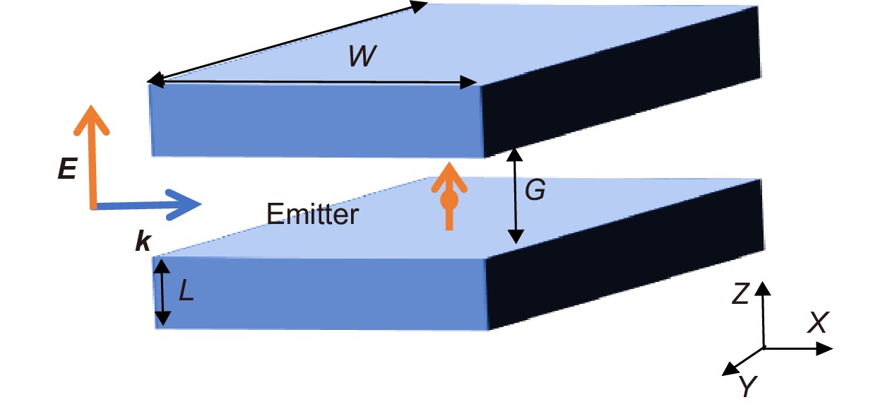
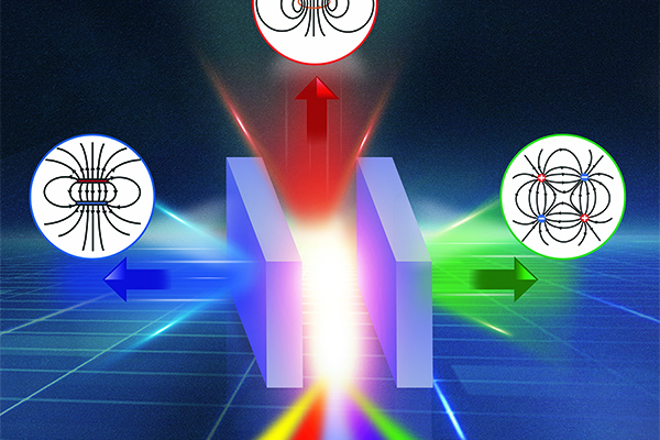
Figure 1.
Schematic of the silicon cuboid dielectric optical nanoantenna.
-
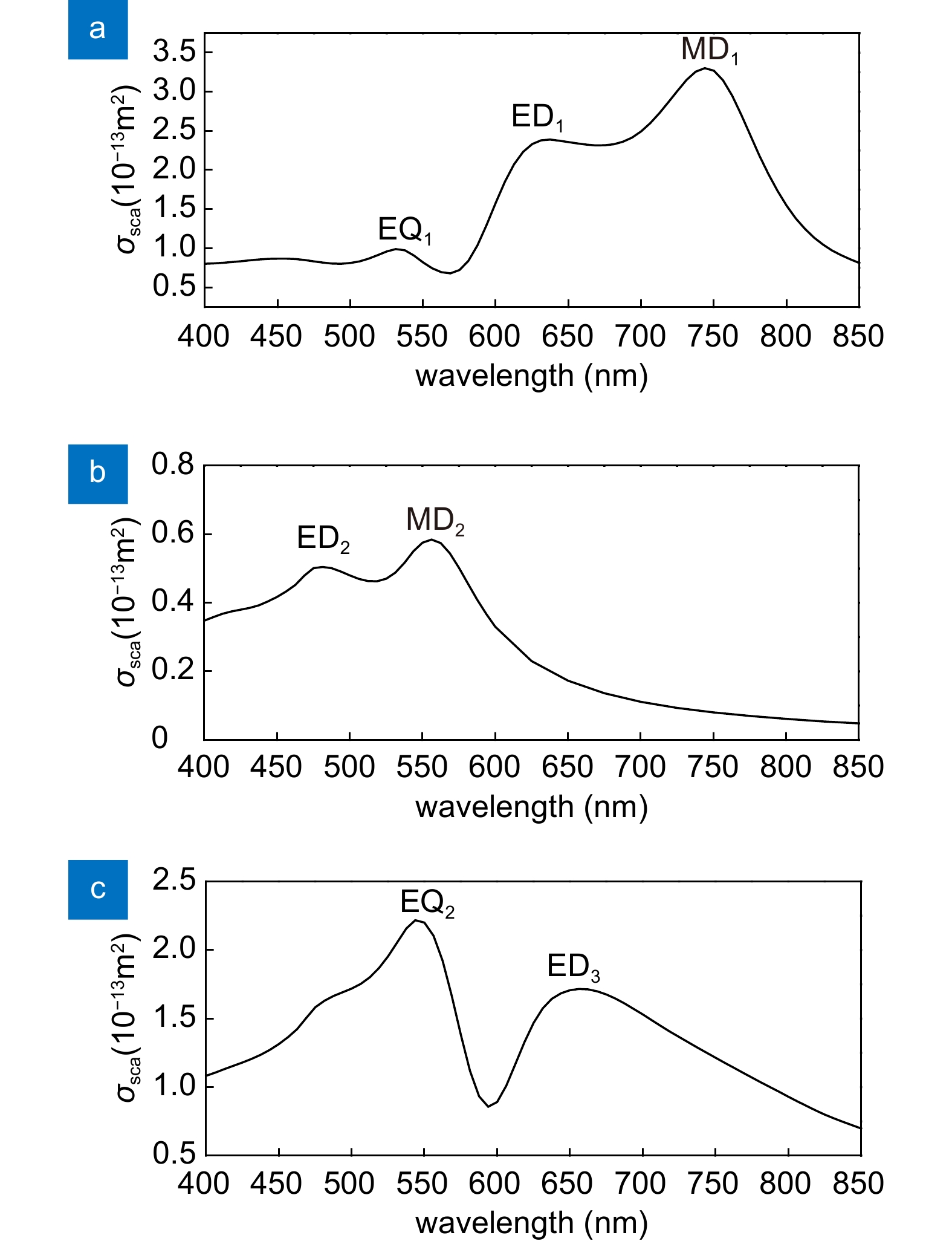
Figure 2.
Calculated scattering cross section for a silicon cuboid nanoantenna with the width W of 220 nm, the length L of 40 nm, and the gap size G of 20 nm upon the plane wave illumination under different plane wave incidence directions and polarizations as follows: (a) Negative y-axis incidence direction and Ex polarization, (b) negative y-axis incidence direction and Ez polarization, and (c) positive z-axis incidence direction and Ey polarization.
-
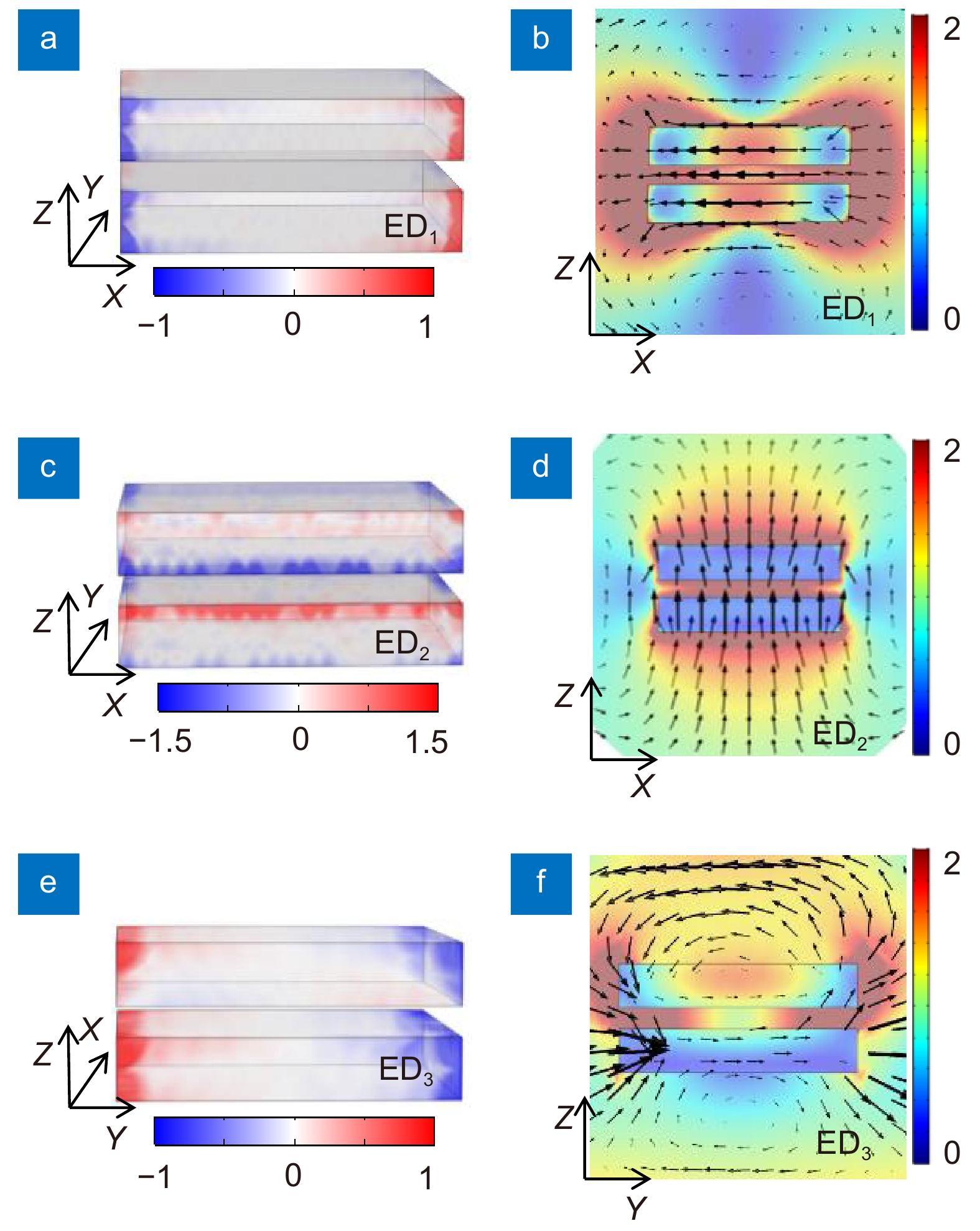
Figure 3.
Polarization charge (ρ) distribution [panels (a), (c) and (e)] and electric field (E) amplitude distribution [panels (b), (d) and (f), color plots] calculated on the specified cutting plane of the nanoantenna at the resonance wavelength of the ED1, ED2 and ED3 mode shown in Fig. 2 respectively. Panel (b) is for the central XZ plane, panel (d) is for the central XZ plane, while panel (f) is for the central YZ plane of the cuboid nanoantenna. The black arrows show the direction of electric field and the length of the arrow denotes the field intensity.
-
Figure 4.
Polarization charge (
$\text{ρ} $ -
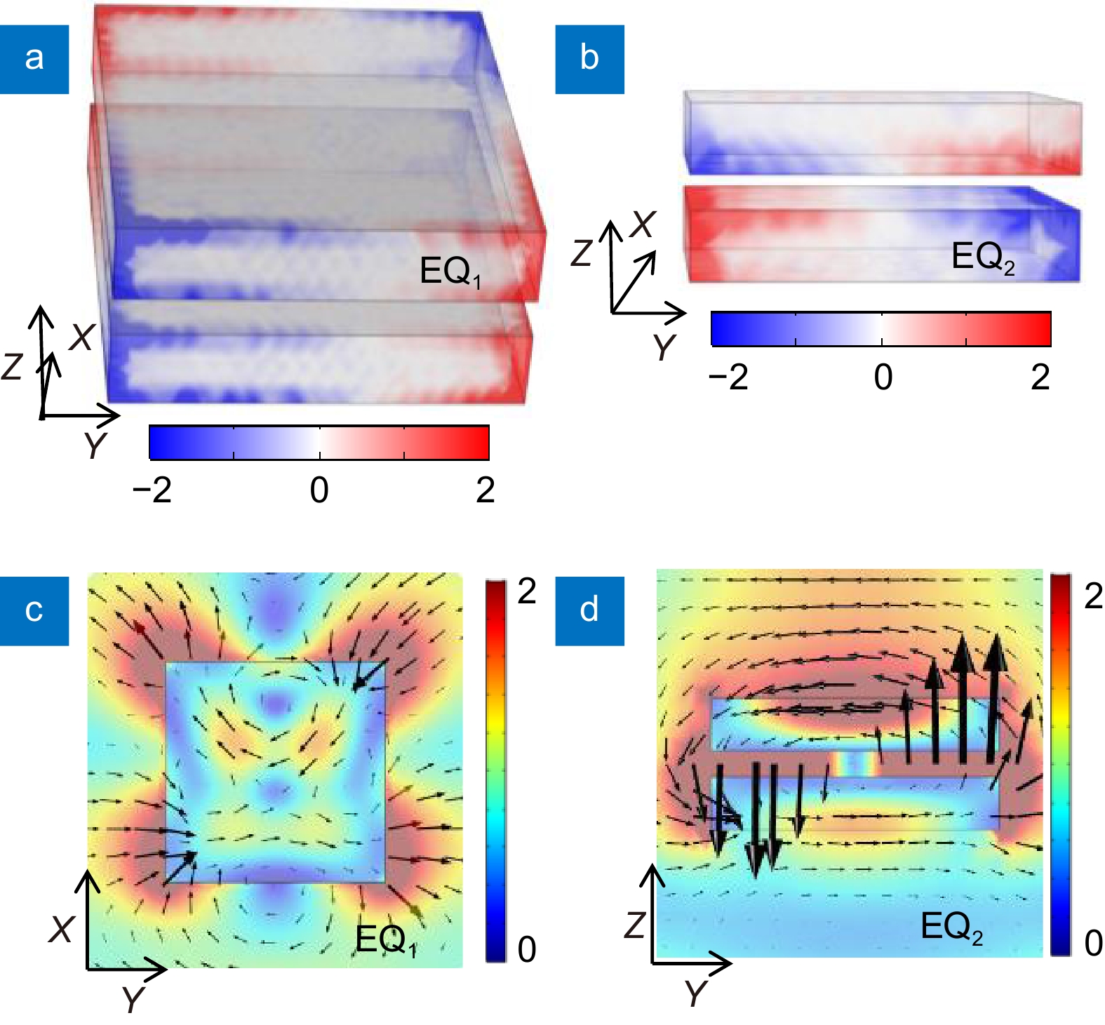
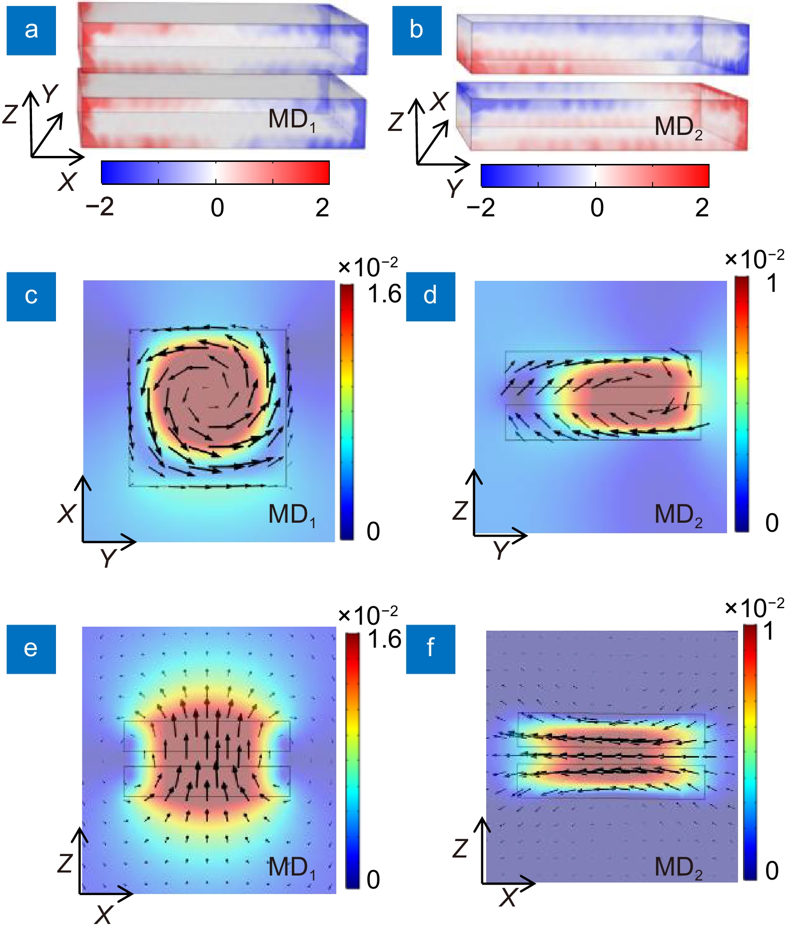
Figure 5.
Polarization charge (
$\text{ρ} $ -
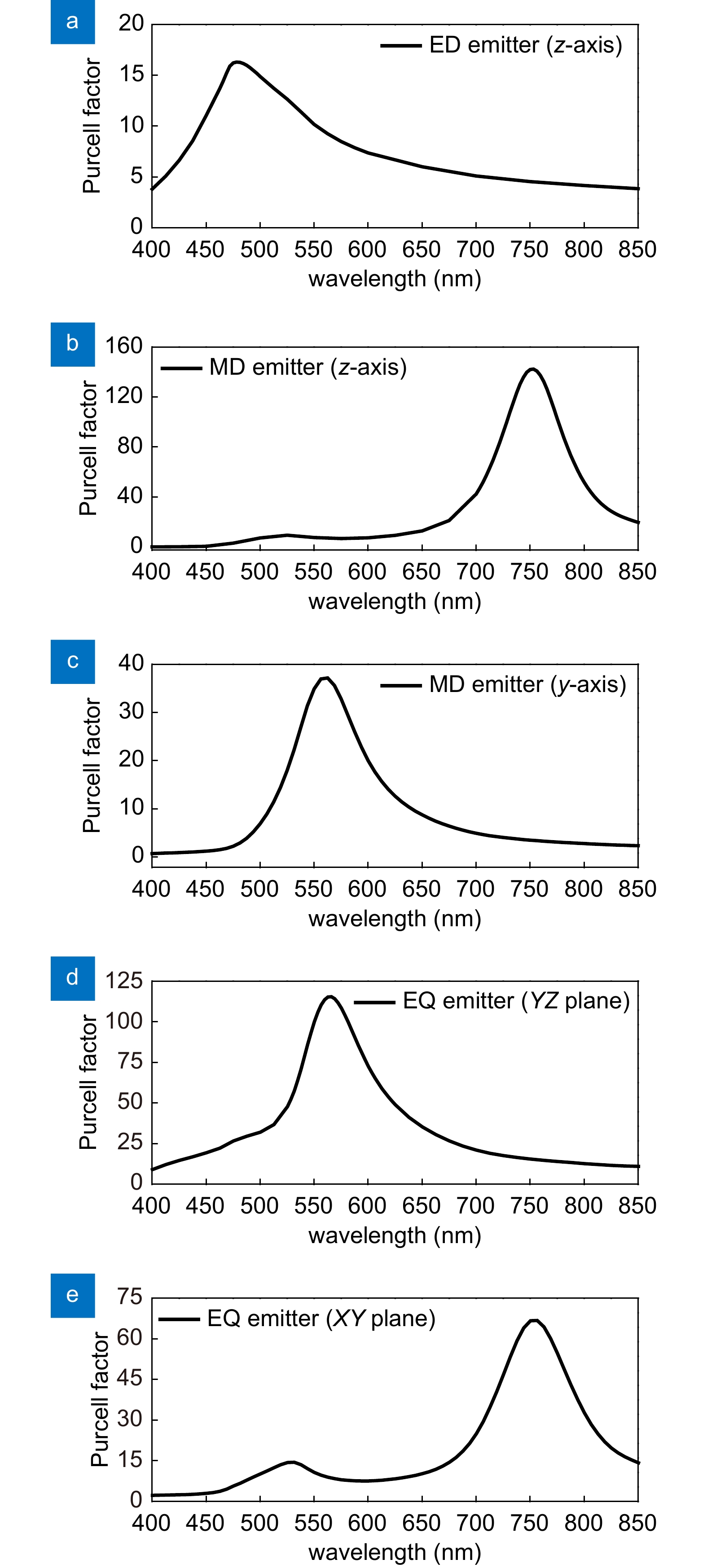
Figure 6.
The radiative decay rate enhancement factors as a function of wavelength for (a) ED, MD [(b) and (d)], and EQ [(c) and (e)] emitter located at the center of the silicon cuboid nanoantenna. The ED emitter has an orientation parallel to the z-axis, the MD emitter has an orientation parallel to the z-axis (b) and x-axis (c), while the EQ emitter has an orientation within the YZ plane(d) and XY plane(e). The width of the cuboid is 220 nm, the length is 40 nm, and the gap size is 20 nm.
-
Figure 7.
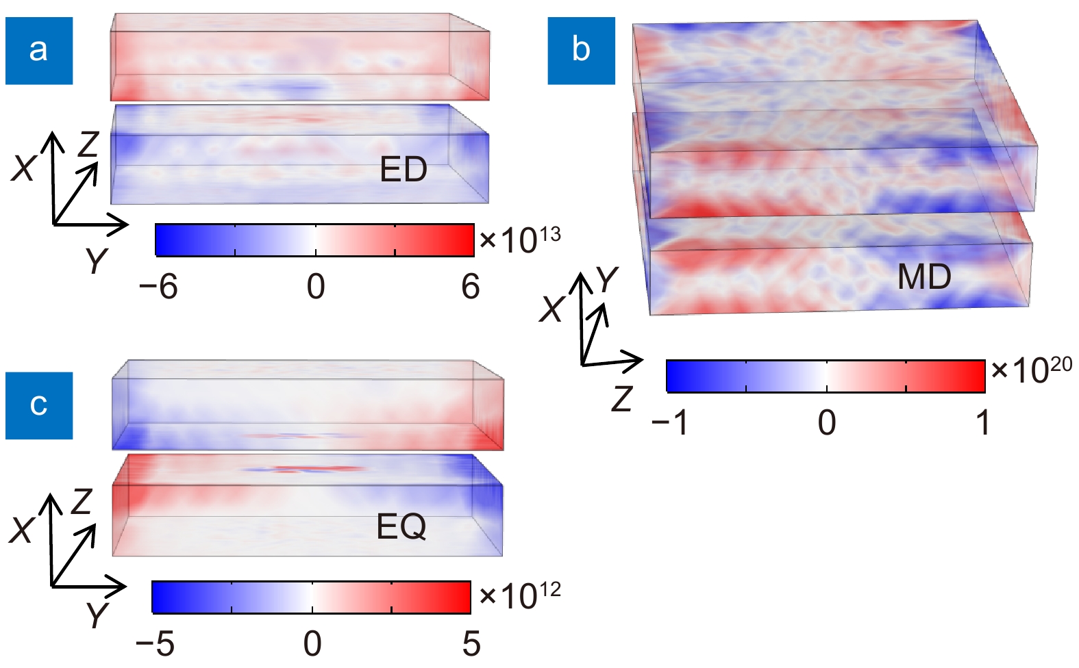
The polarization charge distribution for (a) an ED point emitter oscillating at 475 nm, (b) a MD point emitter oscillating at 750 nm, and (c) an EQ point emitter oscillating at 556 nm. All the emitters are located at the center of the silicon cuboid nanoantenna.
-
Figure FIG. 1302..
cover


