| Citation: | Jiang Z, Fang CZ, Ran X et al. Ultra-high-Q photonic crystal nanobeam cavity for etchless lithium niobate on insulator (LNOI) platform. Opto-Electron Adv 8, 240114 (2025). doi: 10.29026/oea.2025.240114 |
Ultra-high-Q photonic crystal nanobeam cavity for etchless lithium niobate on insulator (LNOI) platform
-
Abstract
The expansive spectral coverage and superior optical properties of lithium niobate (LN) offer a comprehensive suite of tools for exploring novel functionalities. Achieving high-quality (Q) photonic resonator cavities is crucial for enhancing light-matter interactions. However, this task is challenging as the device performance is heavily dependent on the fabrication quality of the LN. In this paper, we present experimental validation of an etchless approach to fabricating high-Q photonic crystal nanobeam cavities (PCNBCs). We successfully fabricate PCNBCs with Q factors exceeding 105 while maintaining high transmittance by capitalizing on the low waveguide loss and high fabrication tolerance of TE-polarized mode. Remarkably, the Q factor achieved here exceeds previous reports on etchless LN PCNBCs by over an order of magnitude. Benefiting from this advancement, we further explore a variety of optical functions, including thermo-optic tuning, optically induced bistability, and Fano line shapes generation. These findings present promising prospects for a versatile platform technique, facilitating the development of high-performance electro-optic or acousto-optic modulators, optical logic devices, and quantum photonics, highlighting its significant impact in the field of photonic integration.-
Keywords:
- photonic crystal nanobeam cavity /
- LNOI platform /
- high Q /
- thermo-optic tuning /
- bistability /
- Fano line shapes
-

-
References
[1] Saleh BEA, Teich MC. Fundamentals of Photonics 3rd ed (John Wiley & Sons, Hoboken, 2019). [2] Vahala KJ. Optical microcavities. Nature 424, 839–846 (2003). [3] Cocorullo G, Della Corte FG, Rendina I et al. Thermo-optic effect exploitation in silicon microstructures. Sens Actuators A Phys 71, 19–26 (1998). [4] Soref RA, Bennett BR. Electrooptical effects in silicon. IEEE J Quantum Electron 23, 123–129 (1987). [5] Shakoor A, Nozaki K, Kuramochi E et al. Compact 1D-silicon photonic crystal electro-optic modulator operating with ultra-low switching voltage and energy. Opt Express 22, 28623–28634 (2014). [6] Abdollahi Shiramin L, Xie WQ, Snyder B et al. High extinction ratio hybrid graphene-silicon photonic crystal switch. IEEE Photonics Technol Lett 30, 157–160 (2018). [7] Zhang Y, He Y, Zhu QM et al. Single-resonance silicon nanobeam filter with an ultra-high thermo-optic tuning efficiency over a wide continuous tuning range. Opt Lett 43, 4518–4521 (2018). [8] Soljačić M, Joannopoulos JD. Enhancement of nonlinear effects using photonic crystals. Nat Mater 3, 211–219 (2004). [9] Chowdhury MZ, Shahjalal M, Ahmed S et al. 6G wireless communication systems: applications, requirements, technologies, challenges, and research directions. IEEE Open J Commun Soc 1, 957–975 (2020). [10] Zhu D, Shao LB, Yu MJ et al. Integrated photonics on thin-film lithium niobate. Adv Opt Photonics 13, 242–352 (2021). [11] Wooten EL, Kissa KM, Yi-Yan A et al. A review of lithium niobate modulators for fiber-optic communications systems. IEEE J Sel Top Quantum Electron 6, 69–82 (2000). [12] Lam CS. A review of the timing and filtering technologies in smartphones. In 2016 IEEE International Frequency Control Symposium (IFCS) 1–6 (IEEE, 2016); http://doi.org/10.1109/FCS.2016.7546724. [13] Suzuki H, Fujiwara M, Iwatsuki K. Application of super-DWDM technologies to terrestrial terabit transmission systems. J Lightwave Technol 24, 1998–2005 (2006). [14] Wang C, Zhang M, Chen X et al. Integrated lithium niobate electro-optic modulators operating at CMOS-compatible voltages. Nature 562, 101–104 (2018). [15] Li MX, Liang HX, Luo R et al. Photon-level tuning of photonic nanocavities. Optica 6, 860–863 (2019). [16] Cai LT, Mahmoud A, Khan M et al. Acousto-optical modulation of thin film lithium niobate waveguide devices. Photonics Res 7, 1003–1013 (2019). [17] Benchabane S, Robert L, Rauch JY et al. Highly selective electroplated nickel mask for lithium niobate dry etching. J Appl Phys 105, 094109 (2009). [18] Geiss R, Diziain S, Steinert M et al. Photonic crystals in lithium niobate by combining focussed ion beam writing and ion-beam enhanced etching. Phys Status Solidi A 211, 2421–2425 (2014). [19] Wu RB, Zhang JH, Yao N et al. Lithium niobate micro-disk resonators of quality factors above 107. Opt Lett 43, 4116–4119 (2018). [20] Gao RH, Zhang HS, Bo F et al. Broadband highly efficient nonlinear optical processes in on-chip integrated lithium niobate microdisk resonators of Q-factor above 108. New J Phys 23, 123027 (2021). [21] Gao RH, Yao N, Guan JL et al. Lithium niobate microring with ultra-high Q factor above 108. Chin Opt Lett 20, 011902 (2022). [22] Yu ZJ, Xi X, Ma JW et al. Photonic integrated circuits with bound states in the continuum. Optica 6, 1342–1348 (2019). [23] Zou CL, Cui JM, Sun FW et al. Guiding light through optical bound states in the continuum for ultrahigh-Q microresonators. Laser Photonics Rev 9, 114–119 (2015). [24] Yu ZJ, Tong YY, Tsang HK et al. High-dimensional communication on etchless lithium niobate platform with photonic bound states in the continuum. Nat Commun 11, 2602 (2020). [25] Ye F, Yu Y, Xi X et al. Second-harmonic generation in etchless lithium niobate nanophotonic waveguides with bound states in the continuum. Laser Photonics Rev 16, 2100429 (2022). [26] Zhang JX, Pan BC, Liu WX et al. Ultra-compact electro-optic modulator based on etchless lithium niobate photonic crystal nanobeam cavity. Opt Express 30, 20839–20846 (2022). [27] Yu ZJ, Sun XK. Acousto-optic modulation of photonic bound state in the continuum. Light Sci Appl 9, 1 (2020). [28] Yu Y, Yu ZJ, Zhang ZY et al. Wavelength-division multiplexing on an etchless lithium niobate integrated platform. ACS Photonics 9, 3253–3259 (2022). [29] Zhang JH, Ma JY, Parry M et al. Spatially entangled photon pairs from lithium niobate nonlocal metasurfaces. Sci Adv 8, eabq4240 (2022). [30] Valencia Molina L, Camacho Morales R, Zhang JH et al. Enhanced infrared vision by nonlinear up-conversion in nonlocal metasurfaces. Adv Mater 36, 2402777 (2024). [31] Čtyroký J, Petráček J, Kuzmiak V et al. Bound modes in the continuum in integrated photonic LiNbO3 waveguides: are they always beneficial. Opt Express 31, 44–55 (2023). [32] Zhang JX, Liu WX, Pan BC et al. High Q Nanobeam cavity based on etchless lithium niobate integrated platform. In 2021 19th International Conference on Optical Communications and Networks (ICOCN) 1–2 (IEEE, 2021); http://doi.org/10.1109/ICOCN53177.2021.9563667. [33] Quan QM, Loncar M. Deterministic design of wavelength scale, ultra-high Q photonic crystal nanobeam cavities. Opt Express 19, 18529–18542 (2011). [34] Quan QM, Deotare PB, Loncar M. Photonic crystal nanobeam cavity strongly coupled to the feeding waveguide. Appl Phys Lett 96, 203102 (2010). [35] Joannopoulos JD, Johnson SG, Winn JN et al. Photonic Crystals: Molding the Flow of Light 2nd ed (Princeton University Press, Princeton, 2008). [36] Li MX, Ling JW, He Y et al. Lithium niobate photonic-crystal electro-optic modulator. Nat Commun 11, 4123 (2020). [37] Zhong H, Zhang RH, He Y et al. Compact photonic crystal nanobeam cavity on Si3N4 Loaded LNOI platform. In 2023 Opto-Electronics and Communications Conference (OECC) 1–2 (IEEE, 2023); http://doi.org/10.1109/OECC56963.2023.10209941. [38] Liang HX, Luo R, He Y et al. High-quality lithium niobate photonic crystal nanocavities. Optica 4, 1251–1258 (2017). [39] Witmer JD, Valery JA, Arrangoiz-Arriola P et al. High-Q photonic resonators and electro-optic coupling using silicon-on-lithium-niobate. Sci Rep 7, 46313 (2017). [40] Wang J, Shen H, Fan L et al. Reconfigurable radio-frequency arbitrary waveforms synthesized in a silicon photonic chip. Nat Commun 6, 5957 (2015). [41] Stern B, Zhu XL, Chen CP et al. On-chip mode-division multiplexing switch. Optica 2, 530–535 (2015). [42] Zhou HY, Qiu CY, Jiang XH et al. Compact, submilliwatt, 2 × 2 silicon thermo-optic switch based on photonic crystal nanobeam cavities. Photonics Res 5, 108–112 (2017). [43] Yu HY, Qiu F. Compact thermo-optic modulator based on a titanium dioxide micro-ring resonator. Opt Lett 47, 2093–2096 (2022). [44] Moretti L, Iodice M, Della Corte FG et al. Temperature dependence of the thermo-optic coefficient of lithium niobate, from 300 to 515 K in the visible and infrared regions. J Appl Phys 98, 036101 (2005). [45] Chen YY, Whitehead J, Ryou A et al. Large thermal tuning of a polymer-embedded silicon nitride nanobeam cavity. Opt Lett 44, 3058–3061 (2019). [46] Quan QM, Burgess IB, Tang SKY et al. High-Q, low index-contrast polymeric photonic crystal nanobeam cavities. Opt Express 19, 22191–22197 (2011). [47] Yao DY, Jiang Z, Zhang Y et al. Ultrahigh thermal-efficient all-optical silicon photonic crystal nanobeam cavity modulator with TPA-induced thermo-optic effect. Opt Lett 48, 2325–2328 (2023). [48] Liu XY, Ying P, Zhong XM et al. Highly efficient thermo-optic tunable micro-ring resonator based on an LNOI platform. Opt Lett 45, 6318–6321 (2020). [49] Li GL, Zheng XZ, Yao J et al. 25Gb/s 1V-driving CMOS ring modulator with integrated thermal tuning. Opt Express 19, 20435–20443 (2011). [50] Gao Y, Zhou W, Sun XK et al. Cavity-enhanced thermo-optic bistability and hysteresis in a graphene-on-Si3N4 ring resonator. Opt Lett 42, 1950–1953 (2017). [51] Almeida VR, Lipson M. Optical bistability on a silicon chip. Opt Lett 29, 2387–2389 (2004). [52] Wen PY, Sanchez M, Gross M et al. Vertical-cavity optical AND gate. Opt Commun 219, 383–387 (2003). [53] Thierfelder C, Sanna S, Schindlmayr A et al. Do we know the band gap of lithium niobate. Phys Status Solidi C 7, 362–365 (2010). [54] Barclay PE, Srinivasan K, Painter O. Nonlinear response of silicon photonic crystal microresonators excited via an integrated waveguide and fiber taper. Opt Express 13, 801–820 (2005). [55] Nozaki K, Shinya A, Matsuo S et al. Ultralow-energy and high-contrast all-optical switch involving Fano resonance based on coupled photonic crystal nanocavities. Opt Express 21, 11877–11888 (2013). [56] Su JY, Huang XQ, Xu HL et al. Ultrafast all-optical switching in a silicon-polymer compound slotted photonic crystal nanobeam cavity. Opt Rev 30, 33–40 (2023). [57] Zheng S, Ruan ZS, Gao SQ et al. Compact tunable electromagnetically induced transparency and Fano resonance on silicon platform. Opt Express 25, 25655–25662 (2017). [58] Guo XQ, Dai TG, Chen B et al. Twin-Fano resonator with widely tunable slope for ultra-high-resolution wavelength monitor. Opt Lett 44, 4527–4530 (2019). [59] Mehta KK, Orcutt JS, Ram RJ. Fano line shapes in transmission spectra of silicon photonic crystal resonators. Appl Phys Lett 102, 081109 (2013). [60] Gu LP, Wang BB, Yuan QC et al. Fano resonance from a one-dimensional topological photonic crystal. APL Photonics 6, 086105 (2021). [61] Galli M, Portalupi SL, Belotti M et al. Light scattering and Fano resonances in high-Q photonic crystal nanocavities. Appl Phys Lett 94, 071101 (2009). [62] Limonov MF, Rybin MV, Poddubny AN et al. Fano resonances in photonics. Nat Photonics 11, 543–554 (2017). -
Access History

Article Metrics
-
Figure 1.
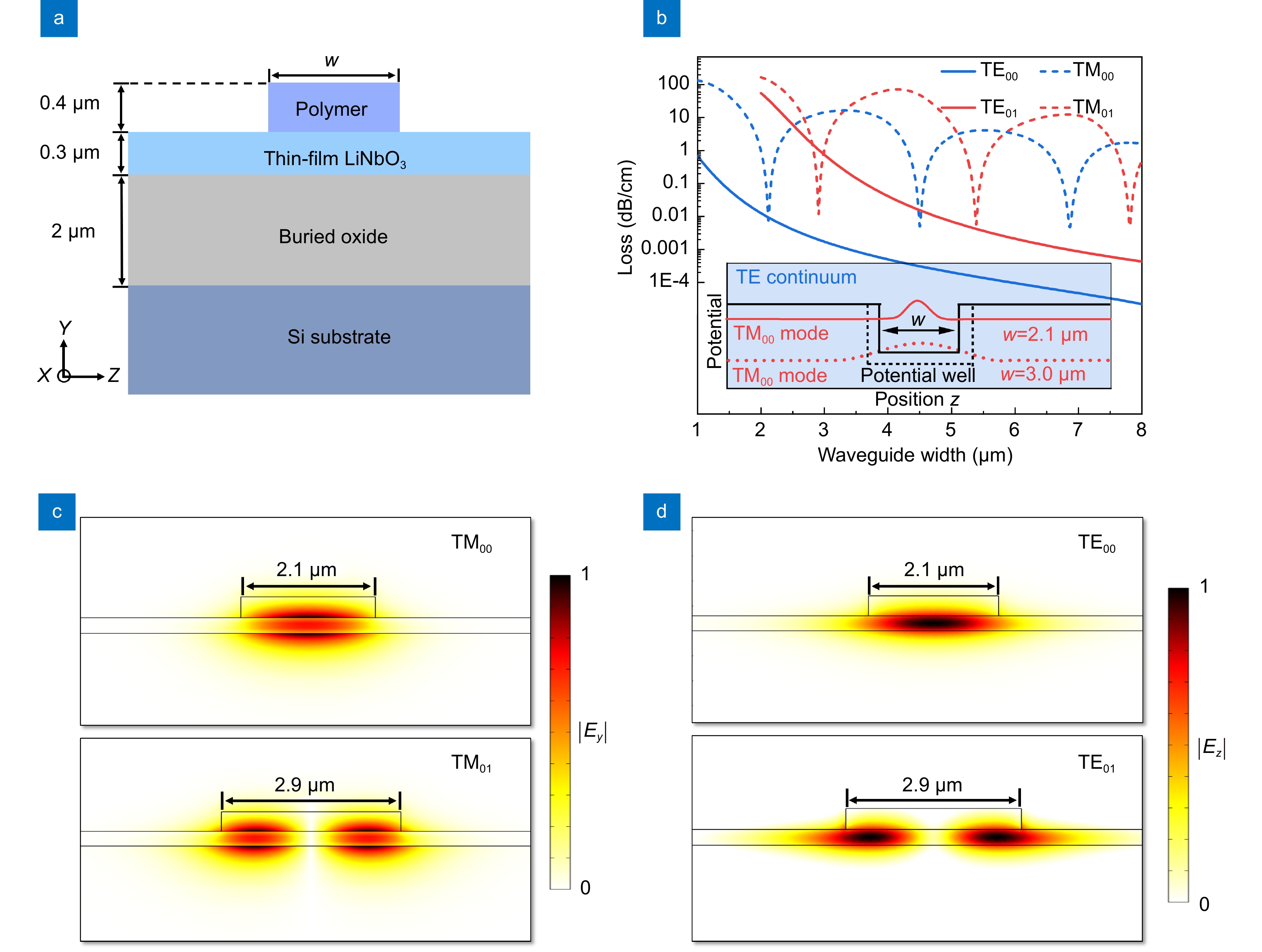
(a) The schematic of the polymer-loaded waveguide. (b) The waveguide loss of different optical modes vs. waveguide width w at 1550 nm. The inset illustrates the photonic potential distribution for the TM00 mode at various waveguide widths. The blue background represents the TE continuum. (c) The electric field (|Ey|) profiles for TM00 and TM01 modes. (d) The electric field (|Ez|) profiles for TE00 and TE01 modes.
-
Figure 2.
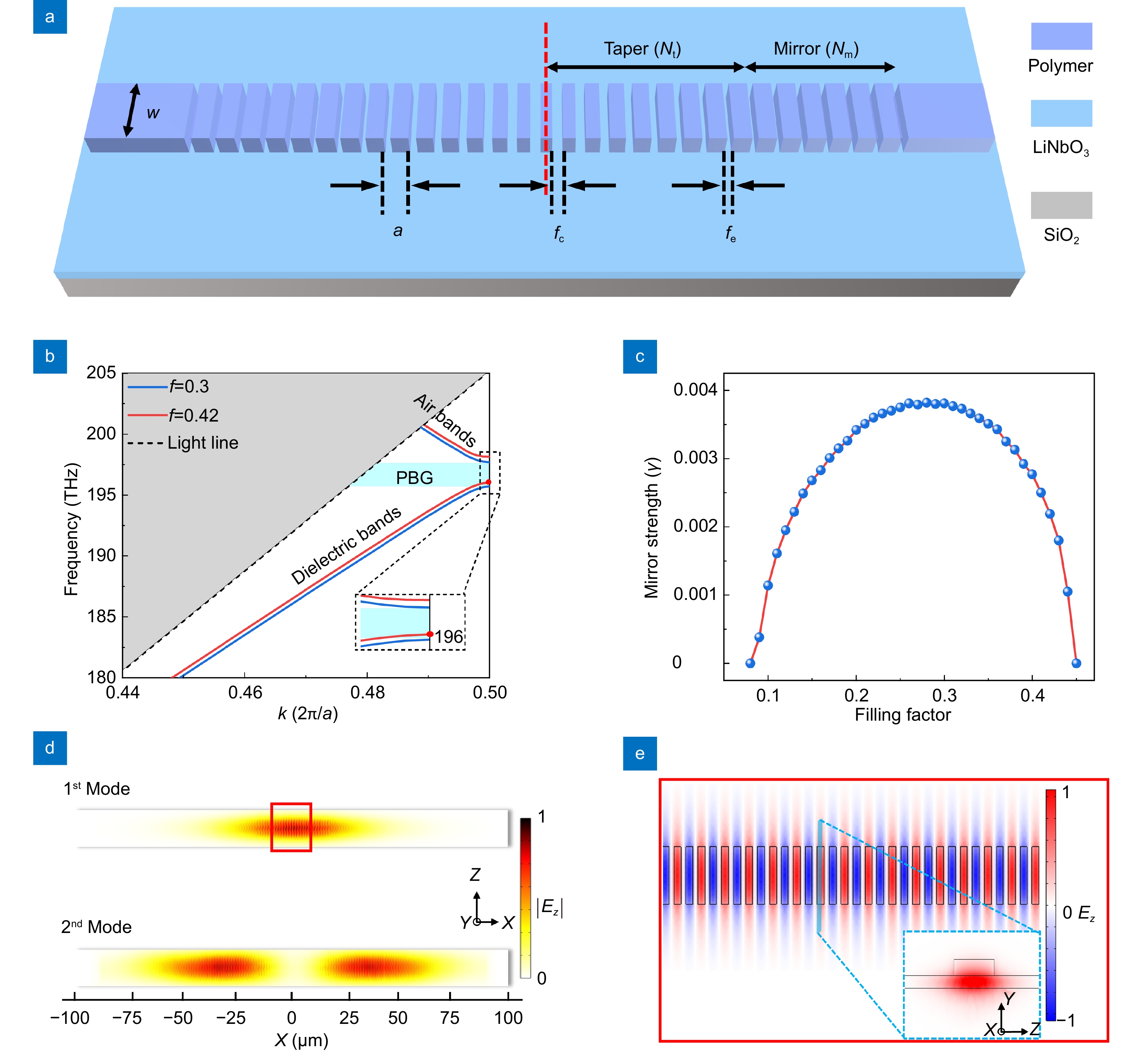
(a) Schematic diagram of the polymer-loaded PCNBC. (b) The band diagram of the TE00 modes for different filling factors: f = 0.3 (blue line) and f = 0.42 (red line). The inset shows the enlarged boxed region and the resonant frequency of the fundamental mode is marked with a red dot. (c) The mirror strength vs. filling factor. (d) The top views of the electric field (|Ez|) profile for the fundamental mode and second-order mode. The orientation of the PCNBC is along the x direction of the LN crystal. (e) Electric field (Ez) distribution profile of the magnified region in (d). The inset shows the electric profile at the y-z plane.
-
Figure 3.
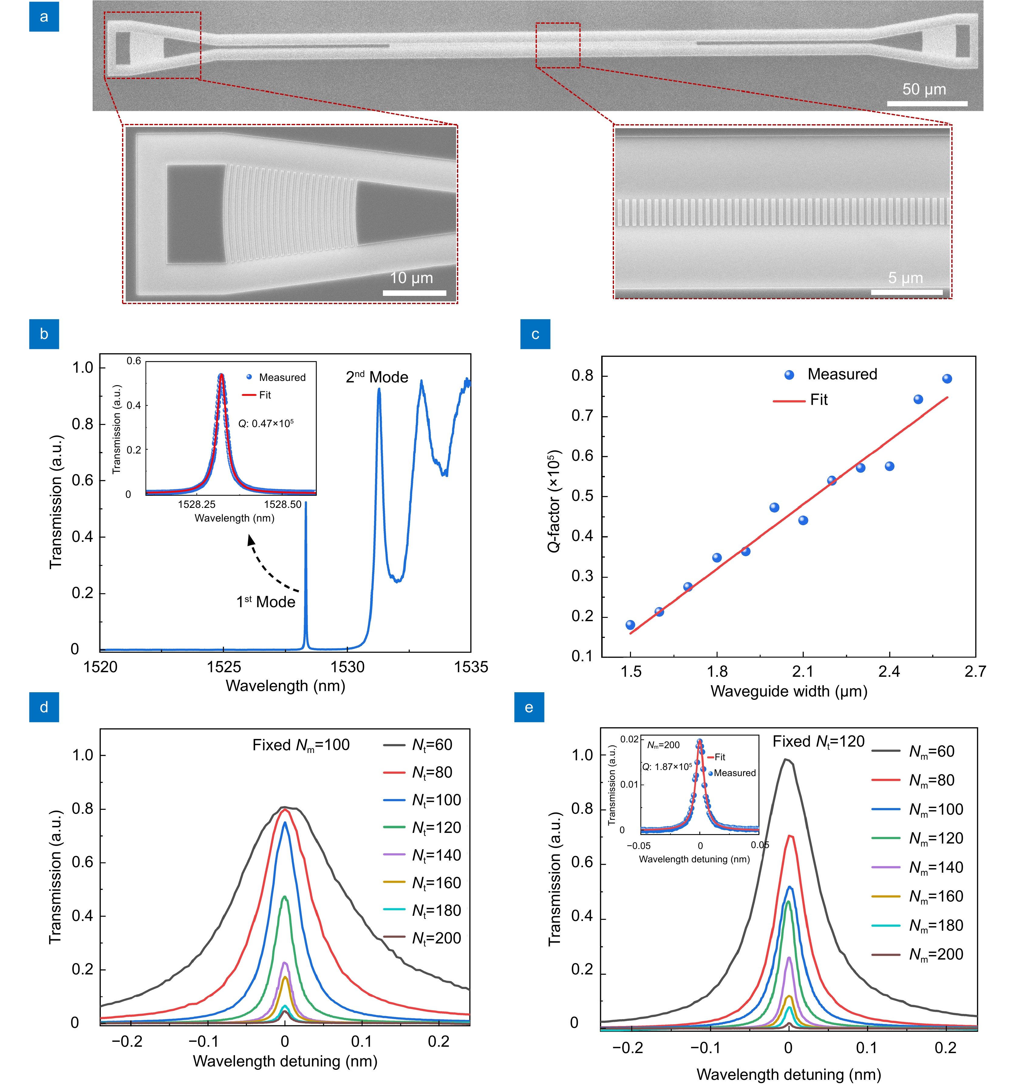
(a) SEM image of the fabricated PCNBC. The bottom insets show the grating coupler (left) and the central region of the cavity (right), respectively. (b) Measured transmission spectrum of a cavity with fc = 0.42, fe = 0.3, Nt = 120, Nm = 100, and w = 2 μm. Inset: the detailed transmission spectrum of the fundamental mode is fitted with a Lorentzian line shape at around 1528.320 nm. (c) Measured Q factors of the fundamental mode vs. waveguide width w. (d) Measured transmission spectra of the fundamental mode for different Nt at Nm = 100. (e) Measured transmission spectra of the fundamental mode for different Nm at Nt = 120. The inset shows the Lorentzian fitting of the transmission spectrum at Nm = 200.
-
Figure 4.
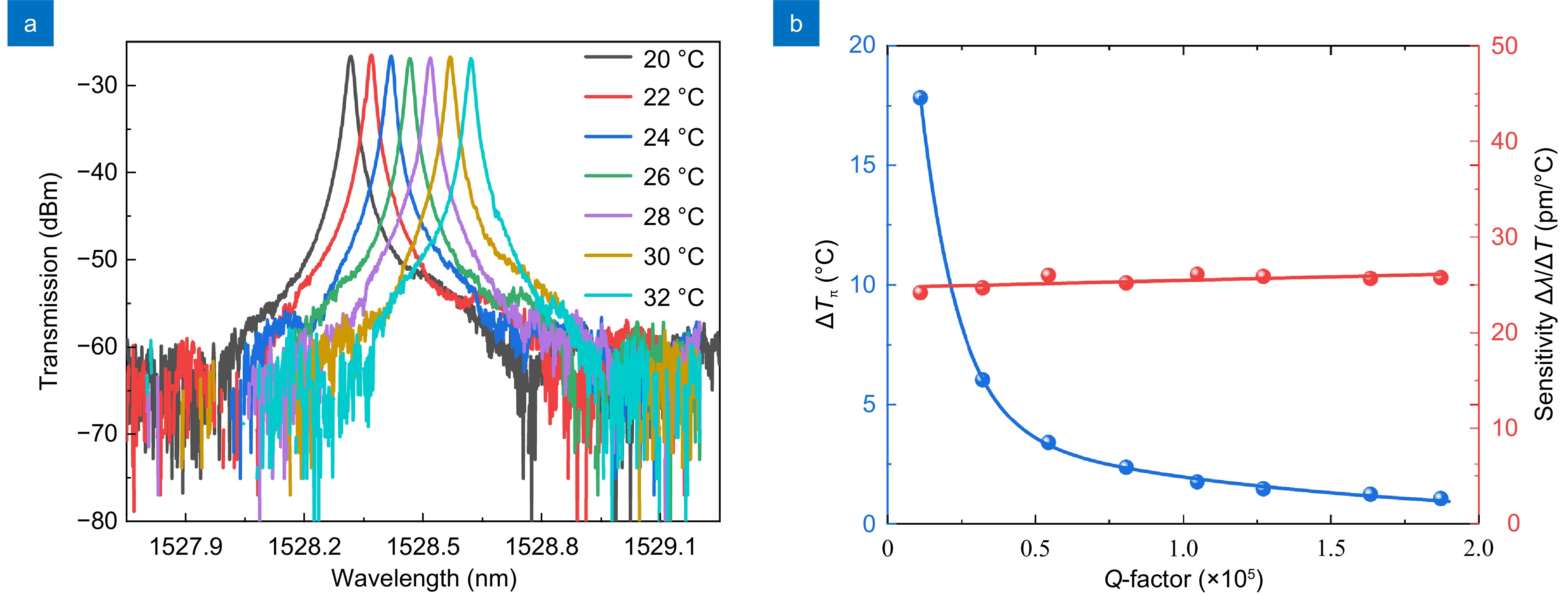
(a) Measured transmission spectra of the PCNBC at different temperatures. The Q factor of the PCNBC is 0.8×10⁵. (b) Measured ΔTπ and the sensitivity of temperature for various devices with different Q factors.
-
Figure 5.
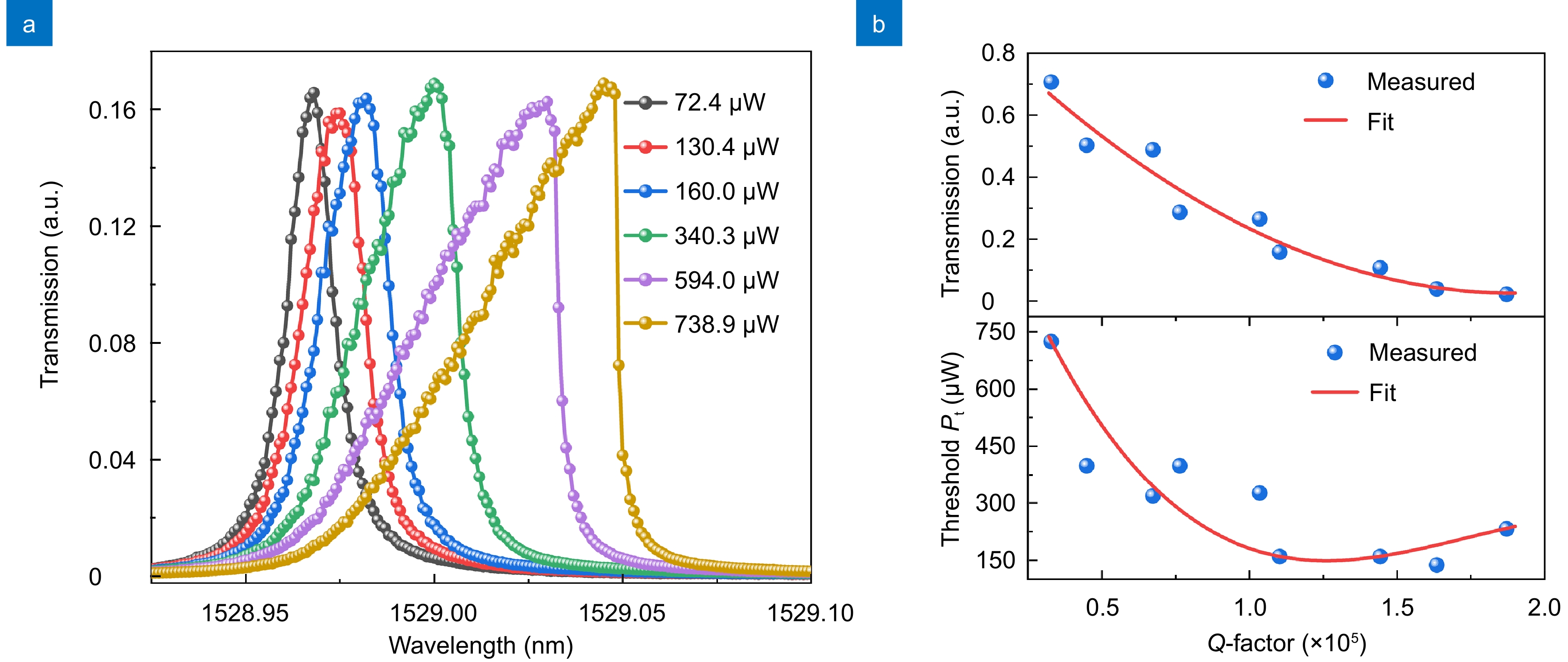
(a) The measured transmission spectra of a PCNBC (Q is 1.04×10⁵) at different input powers. The threshold power is 160 μW. (b) The measured threshold power for the devices with different transmissions and Q factors.
-
Figure 6.
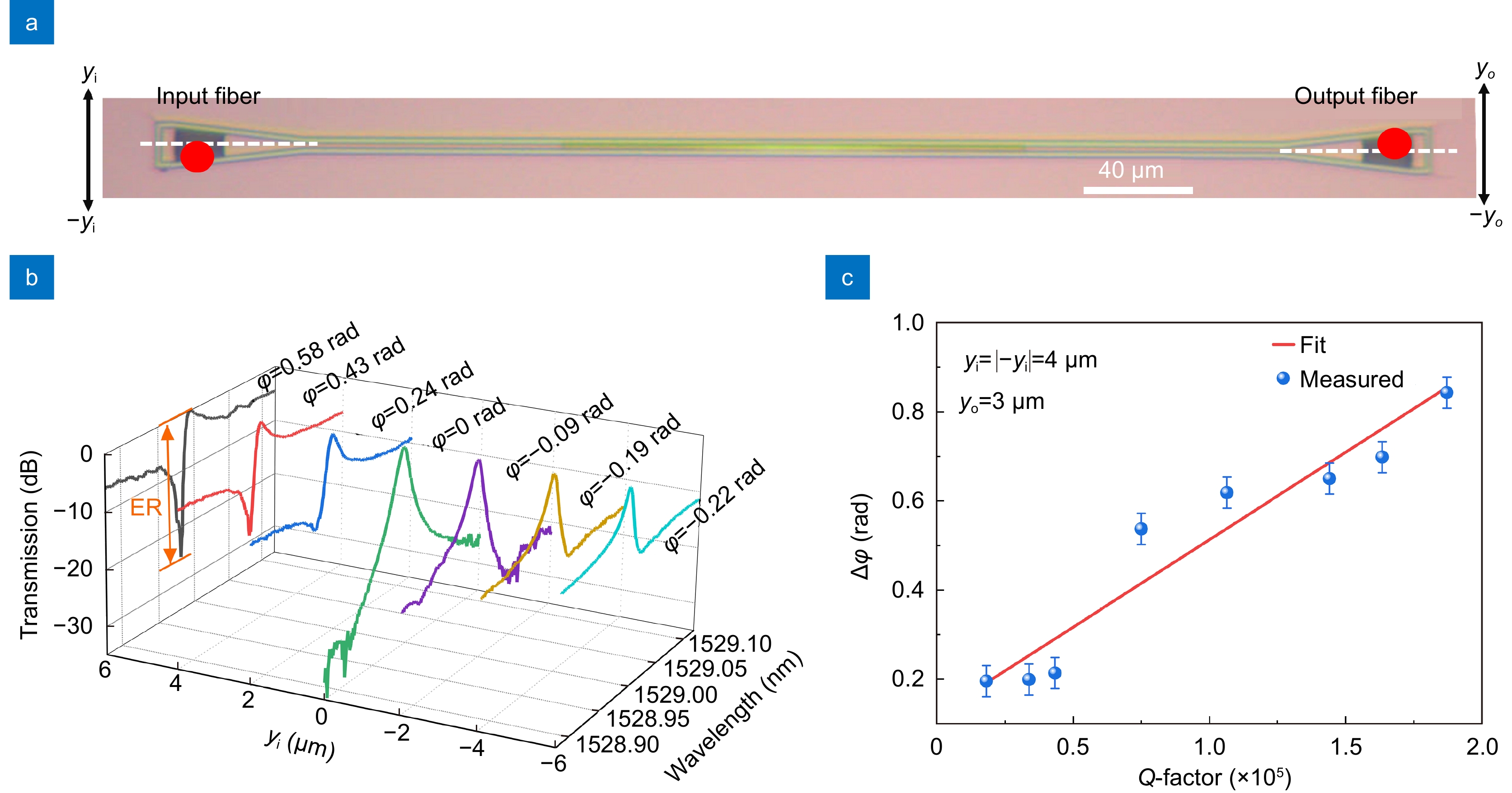
(a) Optical micrograph of the tested PCNBC. The locations of the fibers are indicated by red dots. (b) The measured transmission spectra at different input fiber displacements. The device has a Q of 1.04×10⁵. (c) Devices with different Q factors are measured for Δφ.

 E-mail Alert
 RSS
RSS

 DownLoad:
