| Citation: | Pu MB. Integrated laser processing platform based on metasurface. Opto-Electron Adv 8, 250017 (2025). doi: 10.29026/oea.2025.250017 |
-
Abstract
Laser processing technologies enable the precise fabrication of arbitrary structures and devices with broad applications in micro-optics, micro-mechanics, and biomedicine. However, its adoption is limited by the large size, complexity, high cost, and low flexibility of optical systems. Metasurfaces enable precise multidimensional control of light fields, aligning well with the development trend toward compact, high-performance optical systems. Here, we review several recent studies on the application of metasurfaces in laser processing technologies, including 3D nanolithography, direct laser writing, and laser cutting. Metasurfaces provide an integrated operational platform with exceptional performance, poised to disrupt conventional laser processing workflows. This combination presents significant cost efficiency and substantial development potential, with promising applications in areas such as imaging, optical storage, advanced sensing, and space on-orbit manufacturing.-
Keywords:
- laser processing /
- two-photon polymerization /
- direct laser writing /
- laser cutting /
- metasurface
-

-
References
[1] Chen FY, Shi SX, Xue SY et al. Recent advances and challenges in multi-photon 3D nanoprinting. Engineering (2024), doi: 10.1016/j.eng.2024.09.028. [2] Wang H, Pan CF, Li C et al. Two-photon polymerization lithography for imaging optics. Int J Extreme Manuf 6, 042002 (2024). doi: 10.1088/2631-7990/ad35fe [3] Pinheiro T, Morais M, Silvestre S et al. Direct laser writing: from materials synthesis and conversion to electronic device processing. Adv Mater 36, 2402014 (2024). doi: 10.1002/adma.202402014 [4] Li XR, Zhang BY, Jakobi T et al. Laser-based bionic manufacturing. Int J Extreme Manuf 6, 042003 (2024). doi: 10.1088/2631-7990/ad3f59 [5] Li ZZ, Fan H, Wang L et al. Super-stealth dicing of transparent solids with nanometric precision. Nat Photonics 18, 799–808 (2024). doi: 10.1038/s41566-024-01437-8 [6] Wang XJ, Fang HH, Li ZZ et al. Laser manufacturing of spatial resolution approaching quantum limit. Light Sci Appl 13, 6 (2024). doi: 10.1038/s41377-023-01354-5 [7] Wu CM, Deng HQ, Huang YS et al. Freeform direct-write and rewritable photonic integrated circuits in phase-change thin films. Sci Adv 10, eadk1361 (2024). doi: 10.1126/sciadv.adk1361 [8] Corsetti S, Notaros M, Sneh T et al. Silicon-photonics-enabled chip-based 3D printer. Light Sci Appl 13, 132 (2024). doi: 10.1038/s41377-024-01478-2 [9] Hahn V, Messer T, Bojanowski NM et al. Two-step absorption instead of two-photon absorption in 3D nanoprinting. Nat Photonics 15, 932–938 (2021). doi: 10.1038/s41566-021-00906-8 [10] Hahn V, Rietz P, Hermann F et al. Light-sheet 3D microprinting via two-colour two-step absorption. Nat Photon 16, 784–791 (2022). doi: 10.1038/s41566-022-01081-0 [11] Messer T, Hippe M, Gao JY et al. A shoe-box-sized 3D laser nanoprinter based on two-step absorption. Light Adv Manuf 5, 27 (2024). [12] Gao H, Fan XH, Wang YX et al. Multi-foci metalens for spectra and polarization ellipticity recognition and reconstruction. Opto-Electron Sci 2, 220026 (2023). doi: 10.29026/oes.2023.220026 [13] Ha YL, Luo Y, Pu MB et al. Physics-data-driven intelligent optimization for large-aperture metalenses. Opto-Electron Adv 6, 230133 (2023). doi: 10.29026/oea.2023.230133 [14] Wang QS, Fang Y, Meng Y et al. Vortex-field enhancement through high-threshold geometric metasurface. Opto-Electron Adv 7, 240112 (2024). doi: 10.29026/oea.2024.240112 [15] Xu K, Liu YC, Fan XH et al. Simultaneous dynamic display of meta-hologram and meta-nanoprinting with high frame rate. Laser Photonics Rev 2400815 (2024), doi: 10.1002/lpor.202400815. [16] Liu YC, Xu K, Fan XH et al. Dynamic interactive bitwise meta-holography with ultra-high computational and display frame rates. Opto-Electron Adv 7, 230108 (2024). doi: 10.29026/oea.2024.230108 [17] Wang XE, Fan XH, Liu YC et al. 3D Nanolithography via holographic multi-focus metalens. Laser Photonics Rev 18, 2400181 (2024). doi: 10.1002/lpor.202400181 [18] Fu JC, Jiang MT, Wang Z et al. Supercritical metalens at h-line for high-resolution direct laser writing. Opto-Electron Sci 3, 230035 (2024). doi: 10.29026/oes.2024.230035 [19] Chen BQ, Sun XY, Li XX et al. 4H-SiC metalens: mitigating thermal drift effect in high-power laser irradiation. Adv Mater 37, 2412414 (2025). doi: 10.1002/adma.202412414 -
Access History

Article Metrics
-
Figure 1.
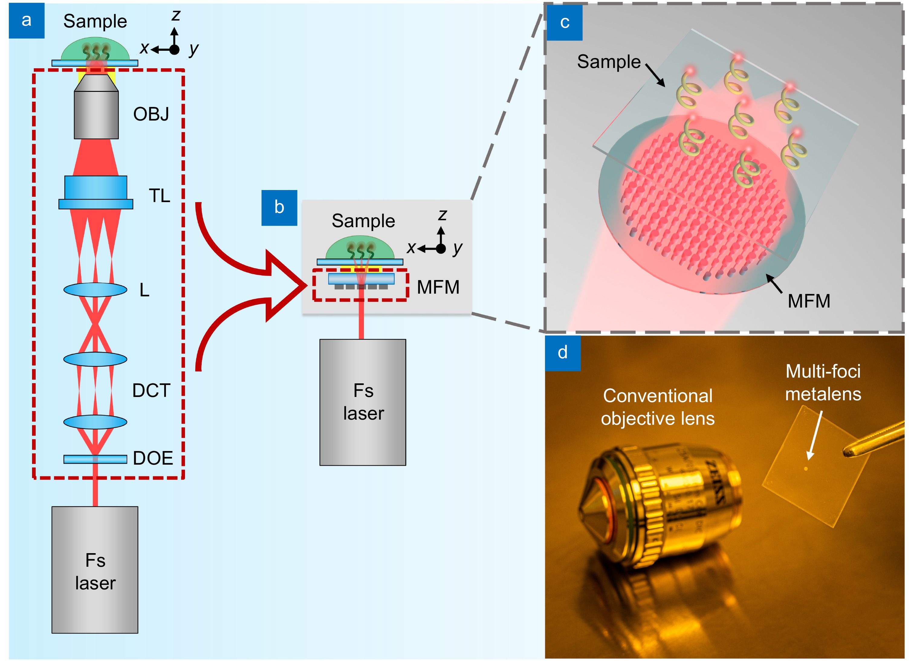
Design concept of M-TPP. (a) Schematic diagram of traditional multi-focus TPP system. (b) Schematic diagram of M-TPP system. (c) Printing process of an array of 3D micro/nanostructures using an MFM. (d) Contrast diagram of the conventional objective lens and the MFM. Figure reproduced from ref.17, John Wiley and Sons.
-
Figure 2.
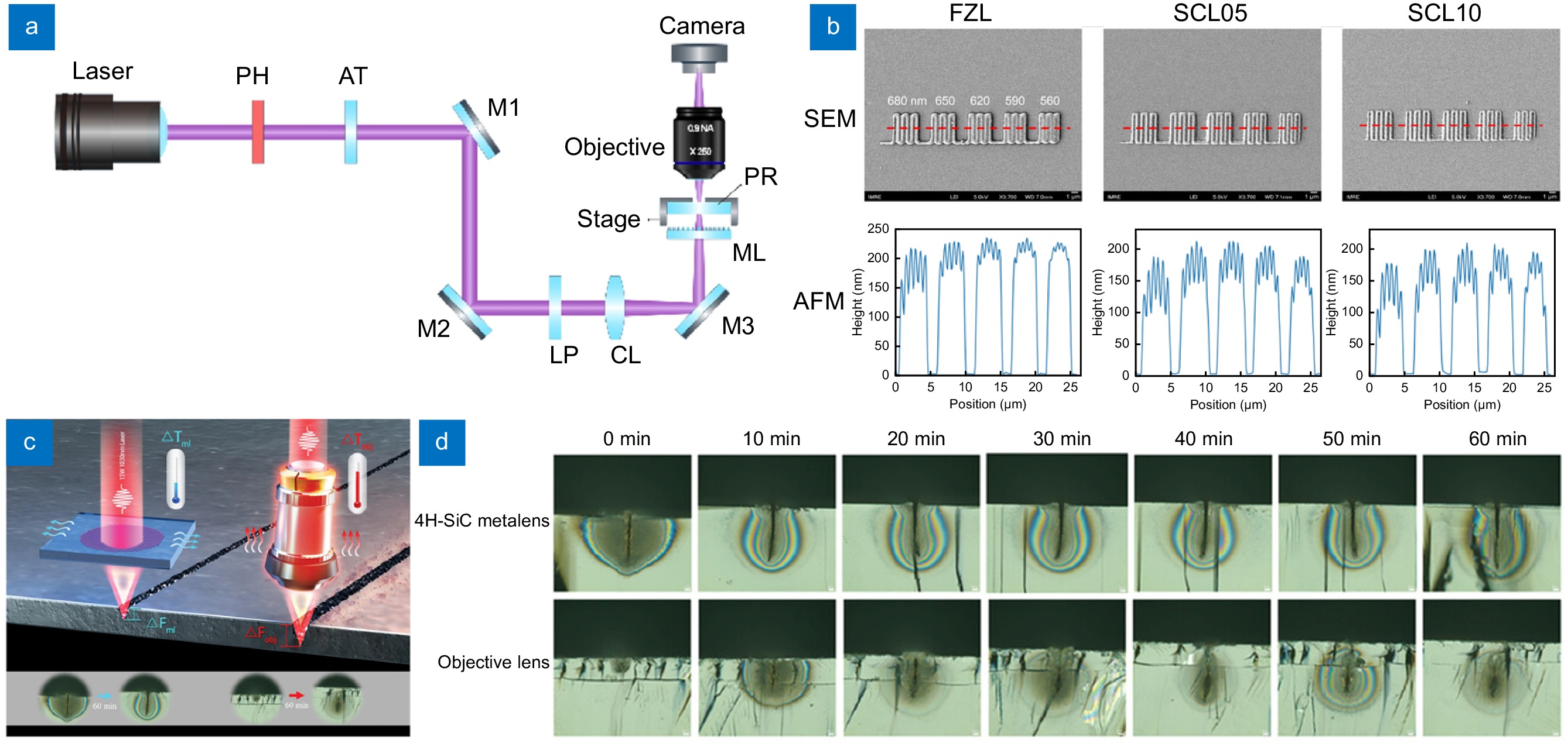
DLW lithography and laser cutting using metalenses. (a) Schematic of the DLW lithography system. (b) Grating patterns produced by DLW with the FZL and the SCLs. (c) Schematic of the thermal drift effects of the SiC metalens (left) and the traditional objective lens (right). (d) Cross-sectional images of 4H-SiC substrates after 60 minutes of laser cutting with a 15 W, 1030 nm laser. Figure reproduced from (a, b) ref.18, under the terms of the Creative Commons CC BY license; (c,d) ref.19, John Wiley and Sons.

 E-mail Alert
 RSS
RSS

 DownLoad:
