2018 Vol. 1, No. 4
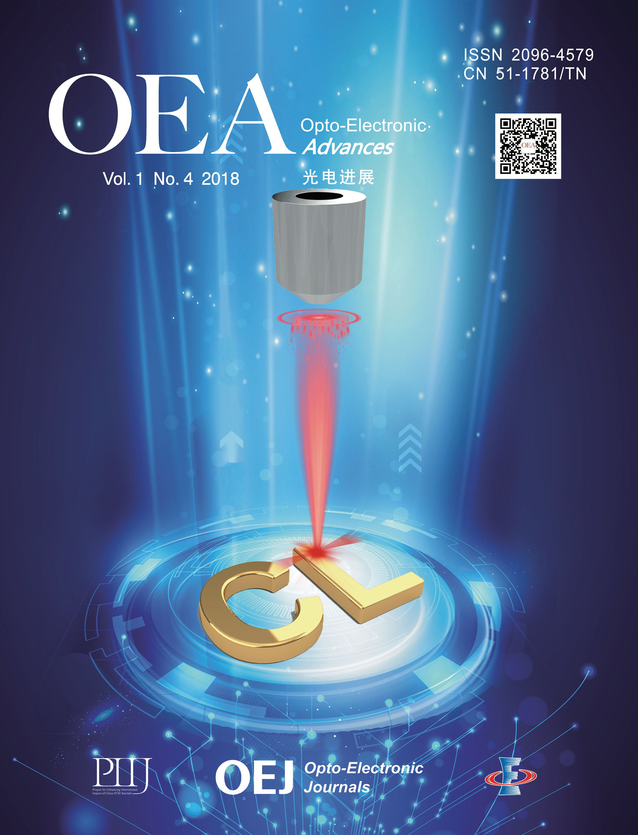
Cover Story: Liu Z X, Jiang M L, Hu Y L, Lin F, Shen B et al. Scanning cathodoluminescence microscopy: applications in semiconductor and metallic nanostructures. Opto-Electron Adv 1, 180007 (2018).
Cathodoluminescence microscopy and spectroscopy with sub-nanoscale resolution, has been successfully used in investigations of quantum phenomena at deep subwavelength. Compared with optical illumination, electron beam excitation has advantages of high energy, deep penetration and large exciting power density, which provides a delicate platform for exploring new phenomena and novel properties of sub-nanostructures. Professor Zheyu Fang’s group in Peking University is devoted to scientific researches of nanophotonics and cathodoluminescence microscopy in recent years. A series of integrated nanofabrication and detecting equipment, including scanning electron microscopy, cathodoluminescence spectroscopy and electron beam lithography, support independent developments related to nanophotonics

-
{{article.year}}, {{article.volume}}({{article.issue}}): {{article.fpage | processPage:article.lpage:6}}. doi: {{article.doi}}{{article.articleStateNameEn}}, Published online {{article.preferredDate | date:'dd MMMM yyyy'}}, doi: {{article.doi}}{{article.articleStateNameEn}}, Accepted Date {{article.acceptedDate | date:'dd MMMM yyyy'}}CSTR: {{article.cstr}}

 E-mail Alert
 RSS
RSS


