
 E-mail Alert
 RSS
RSS2023 Vol. 50, No. 3
Special Issue of Laser Microprocessing & Nanofabrication
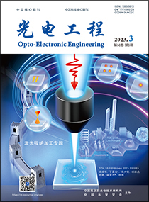
Cover story: Yang S H, Ding C L, Zhu D Z, et al. High-speed two-photon lithography based on femtosecond laser[J]. Opto-Electron Eng, 2023, 50(3): 220133
The femtosecond laser has become a research hotspot in the micro and nano processing field for its unique interaction mechanism with materials due to its haracteristics of ultra-short pulse width and ultra-high peak power density. And the femtosecond two-photon lithography (TPL) is highly desirable in various emerging fields such as photonic chips, micro-sensors, on-chip artificial intelligence, etc. for its advantages of maskless lithography, 3D processing capacity, etc. However, comparing with the widely-used exposure lithography, the application of TPL technology in other fields is severely restricted.
The research team led by Professor Liu Xu and Professor Kuang Cuifang aim at the femtosecond TPL efficiency and summarize the research works on the efficiency improvement. They firstly present the single-beam writing method frequently used in TPL. Then sequentially introduce the multi-foci parallel lithography, which can obviously promote the writing efficiency by generating dozens or even hundreds of thousands of foci. Comprehensively summarizes the research progress of two-photon direct writing technology in improving efficiency, including the single-beam writing based on various high-speed scanning devices, multi-focus parallel writing based on interference lattice, MLA, DOE, SLM and DMD, 2D pattern projection based on SLM/DMD, and 3D exposure technology based on SLM, etc.
Special Issue of Laser Microprocessing & Nanofabrication
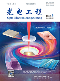
Back cover story: Dong B, Zhang J, Wang D W, et al. Femtosecond laser micromachining optical devices[J]. Opto-Electron Eng, 2023, 50(3): 220073
Currently, the development of semiconductor technology based on electrons has reached its physical limit. The information technology based on photons stands out for its fast response, high information capacity, excellent parallel processing ability and low power consumption. Compared with traditional long-pulse or continuous laser processing technology, femtosecond laser exhibits various advantages such as ultrashort pulse width, ultrahigh peak power and ultralow thermal effect, thus making itself a more advanced micro/nano processing tool.
The team of Professor Wu Dong from University of Science and Technology of China review the principle, advantage and technique of femtosecond laser micromachining and its application in fabricating optical devices were discussed in detail. The contradiction between resolution and the effective processing range in femtosecond laser micromachining, as well as various techniques to improve the resolution was emphasized. Then they focused on various femtosecond laser processing techniques and their various applications in the fabrication of micro/nano optical devices.
Although researchers have been exploring the application of femtosecond laser micromachining optical devices and made lots of progress, the relevant research is still not systematic. how to integrate various optical devices onto a single photonic chip still faces various challenges, such as realizing the packaging of various optical devices on the same substrate, avoiding crosstalk between different optical devices, and efficient conversion of opto-electronic signals.

-
{{article.year}}, {{article.volume}}({{article.issue}}): {{article.fpage | processPage:article.lpage:6}}. doi: {{article.doi}}{{article.articleStateNameEn}}, Published online {{article.preferredDate | date:'dd MMMM yyyy'}}, doi: {{article.doi}}{{article.articleStateNameEn}}, Accepted Date {{article.acceptedDate | date:'dd MMMM yyyy'}}CSTR: {{article.cstr}}
Prof. Xiangang Luo


