| Citation: | Xu K, Huang PL, Huang LY et al. High-precision multi-focus laser sculpting of microstructured glass. Opto-Electron Adv 7, 240082 (2024). doi: 10.29026/oea.2024.240082 |
High-precision multi-focus laser sculpting of microstructured glass
-
Abstract
Precision sculpting of glass with defined surface microstructures is vital due to the miniaturization and integration of glass-based devices, while it is still challenging as the high brittleness of glass. We here create a three-dimensional multi-focus laser for glass micro-sculpting through a beam-shaping technology based on the superposition of lens and grating phase diagrams. The multi-focus laser modification in tandem with chemical etching enables the fabrication of glass microstructures with highly adjustable profiles. Refractive-index-induced deviations are migrated via algorithm correction to ensure multi-focus positional accuracy. Energy un-uniformity due to equidistant laser spots arrangement is eliminated through their coordinate randomization following the target profiles. Finally, uniform laser spots with a proper point-to-point distance create connected cracks inside glass, enabling efficient etching with enhanced rates along the modified profile and the fabrication of surface microstructures. We demonstrate diverse groove arrays with profiles of trapezoid, semicircle, and triangle, revealing low roughness around 1.3 μm, a high depth-width ratio of 3:1, and depth up to 300 μm, which underscore broad applications such as fiber packaging.-
Keywords:
- ultrafast laser processing /
- multi-focus shaping beam /
- micro-groove /
- glass
-

-
References
[1] Luo Z, Yin K, Dong XR et al. Fabrication of parabolic cylindrical microlens array by shaped femtosecond laser. Opt Mater 78, 465–470 (2018). doi: 10.1016/j.optmat.2018.03.003 [2] Yuan W, Li LH, Lee WB et al. Fabrication of microlens array and its application: a review. Chin J Mech Eng 31, 16 (2018). doi: 10.1186/s10033-018-0204-y [3] Ha TW, Heo GS, Choi BH et al. Wafer-level fabrication of a high-silica v-groove for fiber-optic packaging using deep dry-etching with a dual-frequency high-density plasma. J Korean Phys Soc 67, 1179–1186 (2015). doi: 10.3938/jkps.67.1179 [4] Gottmann J, Hermans M, Repiev N et al. Selective laser-induced etching of 3D precision quartz glass components for microfluidic applications—up-scaling of complexity and speed. Micromachines 8, 110 (2017). doi: 10.3390/mi8040110 [5] Xiong JH, Hsiang EL, He ZQ et al. Augmented reality and virtual reality displays: emerging technologies and future perspectives. Light Sci Appl 10, 216 (2021). doi: 10.1038/s41377-021-00658-8 [6] Wen XW, Zhang BY, Wang WP et al. 3D-printed silica with nanoscale resolution. Nat Mater 20, 1506–1511 (2021). doi: 10.1038/s41563-021-01111-2 [7] Toombs JT, Luitz M, Cook CC et al. Volumetric additive manufacturing of silica glass with microscale computed axial lithography. Science 376, 308–312 (2022). doi: 10.1126/science.abm6459 [8] Zhou TF, Liu XH, Liang ZQ et al. Recent advancements in optical microstructure fabrication through glass molding process. Front Mech Eng 12, 46–65 (2017). doi: 10.1007/s11465-017-0425-2 [9] Zhou TF, He YP, Wang TX et al. A review of the techniques for the mold manufacturing of micro/nanostructures for precision glass molding. Int J Extrem Manuf 3, 042002 (2021). doi: 10.1088/2631-7990/ac1159 [10] Zhang B, Wang Z, Tan DZ et al. Ultrafast laser-induced self-organized nanostructuring in transparent dielectrics: fundamentals and applications. PhotoniX 4, 24 (2023). doi: 10.1186/s43074-023-00101-8 [11] Wang Z, Zhang B, Wang ZQ et al. 3D imprinting of voxel-level structural colors in lithium niobate crystal. Adv Mater 35, 2303256 (2023). doi: 10.1002/adma.202303256 [12] Luo Z, Duan J, Guo CL. Femtosecond laser one-step direct-writing cylindrical microlens array on fused silica. Opt Lett 42, 2358–2361 (2017). doi: 10.1364/OL.42.002358 [13] Pan A, Chen T, Li CX et al. Parallel fabrication of silicon concave microlens array by femtosecond laser irradiation and mixed acid etching. Chin Opt Lett 14, 052201 (2016). doi: 10.3788/COL201614.052201 [14] Liesener J, Reicherter M, Haist T et al. Multi-functional optical tweezers using computer-generated holograms. Opt Commun 185, 77–82 (2000). doi: 10.1016/S0030-4018(00)00990-1 [15] Zhou C, Liu L. Numerical study of dammann array illuminators. Appl Opt 34, 5961–5969 (1995). doi: 10.1364/AO.34.005961 [16] Yang GZ, Dong BZ, Gu BY et al. Gerchberg–Saxton and Yang–Gu algorithms for phase retrieval in a nonunitary transform system: a comparison. Appl Opt 33, 209–218 (1994). doi: 10.1364/AO.33.000209 [17] Takahashi H, Hasegawa S, Hayasaki Y. Holographic femtosecond laser processing using optimal-rotation-angle method with compensation of spatial frequency response of liquid crystal spatial light modulator. Appl Opt 46, 5917–5923 (2007). doi: 10.1364/AO.46.005917 [18] Wang L, Gong W, Cao XW et al. Holographic laser fabrication of 3D artificial compound μ-eyes. Light Adv Manuf 4, 26 (2023). [19] Lesem LB, Hirsch PM, Jordan JA. The kinoform: a new wavefront reconstruction device. IBM J Res Dev 13, 150–155 (1969). doi: 10.1147/rd.132.0150 [20] Curtis JE, Schmitz CHJ, Spatz JP. Symmetry dependence of holograms for optical trapping. Opt Lett 30, 2086–2088 (2005). doi: 10.1364/OL.30.002086 [21] Jesacher A, Booth MJ. Parallel direct laser writing in three dimensions with spatially dependent aberration correction. Opt Express 18, 21090–21099 (2010). doi: 10.1364/OE.18.021090 [22] Chen F, Liu HW, Yang Q et al. Maskless fabrication of concave microlens arrays on silica glasses by a femtosecond-laser-enhanced local wet etching method. Opt Express 18, 20334–20343 (2010). doi: 10.1364/OE.18.020334 [23] Wu PC, Cao XW, Chen ZH et al. Fabrication of cylindrical microlens by femtosecond laser-assisted hydrofluoric acid wet etching of fused silica. Adv Photonics Res 4, 2200227 (2023). doi: 10.1002/adpr.202200227 [24] Kim S, Kim J, Joung YH et al. Optimization of selective laser-induced etching (SLE) for fabrication of 3D glass microfluidic device with multi-layer micro channels. Micro Nano Syst Lett 7, 15 (2019). doi: 10.1186/s40486-019-0094-5 [25] Bischof D, Kahl M, Michler M. Laser-assisted etching of borosilicate glass in potassium hydroxide. Opt Mater Express 11, 1185–1195 (2021). doi: 10.1364/OME.417871 [26] Pedrotti FL, Pedrotti LM, Pedrotti LS. Introduction to Optics 3rd ed (Cambridge University Press, Cambridge, 2017). [27] Huang LY, Xu K, Yuan DD et al. Sub-wavelength patterned pulse laser lithography for efficient fabrication of large-area metasurfaces. Nat Commun 13, 5823 (2022). doi: 10.1038/s41467-022-33644-8 -
Supplementary Information
Supplementary information for High-precision multi-focus laser sculpting of microstructured glass 
-
Access History

Article Metrics
-
Figure 1.
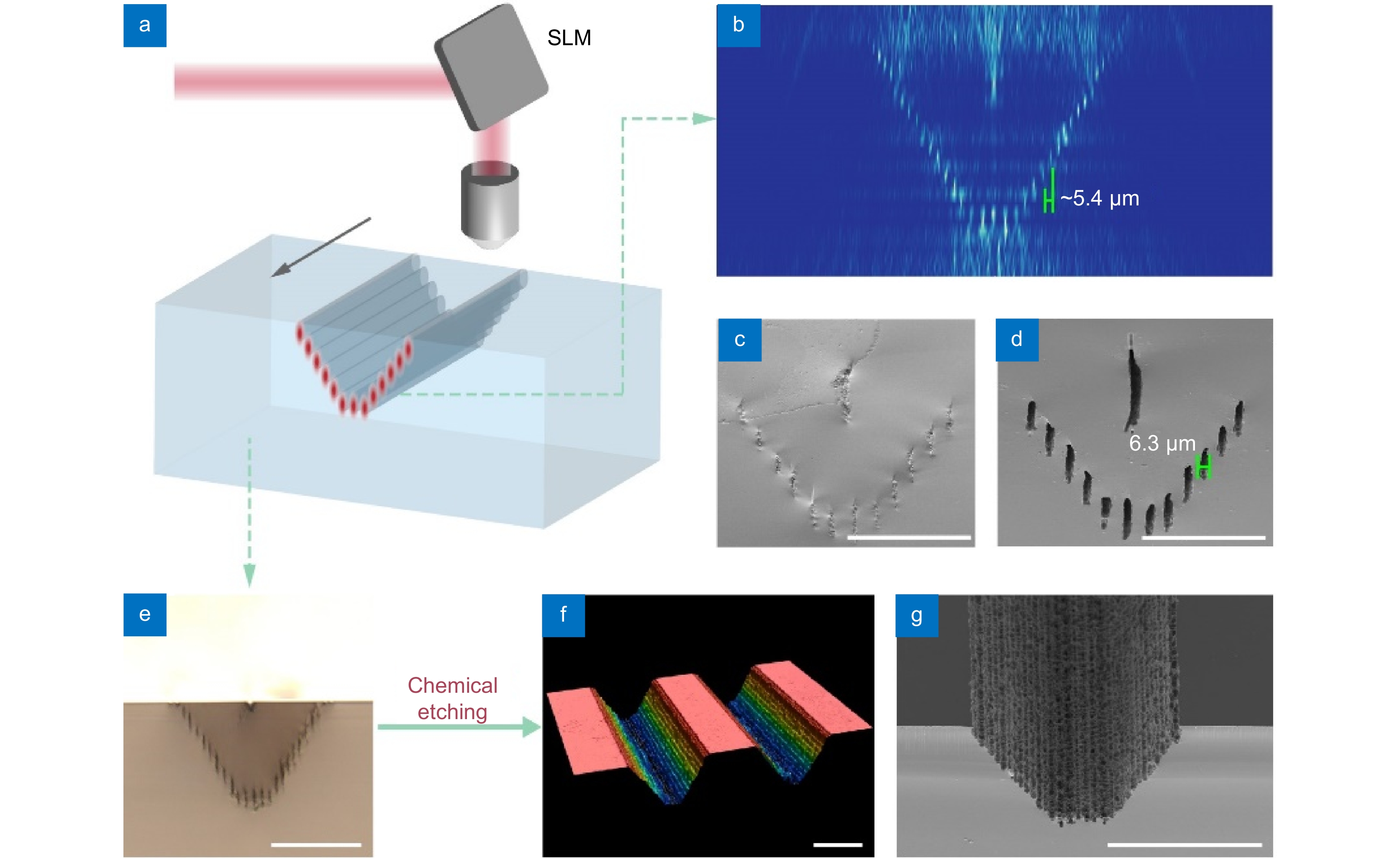
Multi-focus laser processing for efficient fabrication of a trapezoid groove. (a) Schematic of multi-focus laser processing. (b) Simulated light intensity field of multi-focus spot. (c) 45° tilted view of multi-focus ablation. (d) 45° tilted view of multi-focus ablation after chemical etching. (e) Cross-sectional view of the groove on fused silica after laser processing, observed with an optical microscope. (f) Three-dimensional view of the groove after chemical etching, captured by laser scanning confocal microscopy. (g) 45° tilted view of the groove, imaged with scanning electronic microscope. Scale bars: 100 μm.
-
Figure 2.
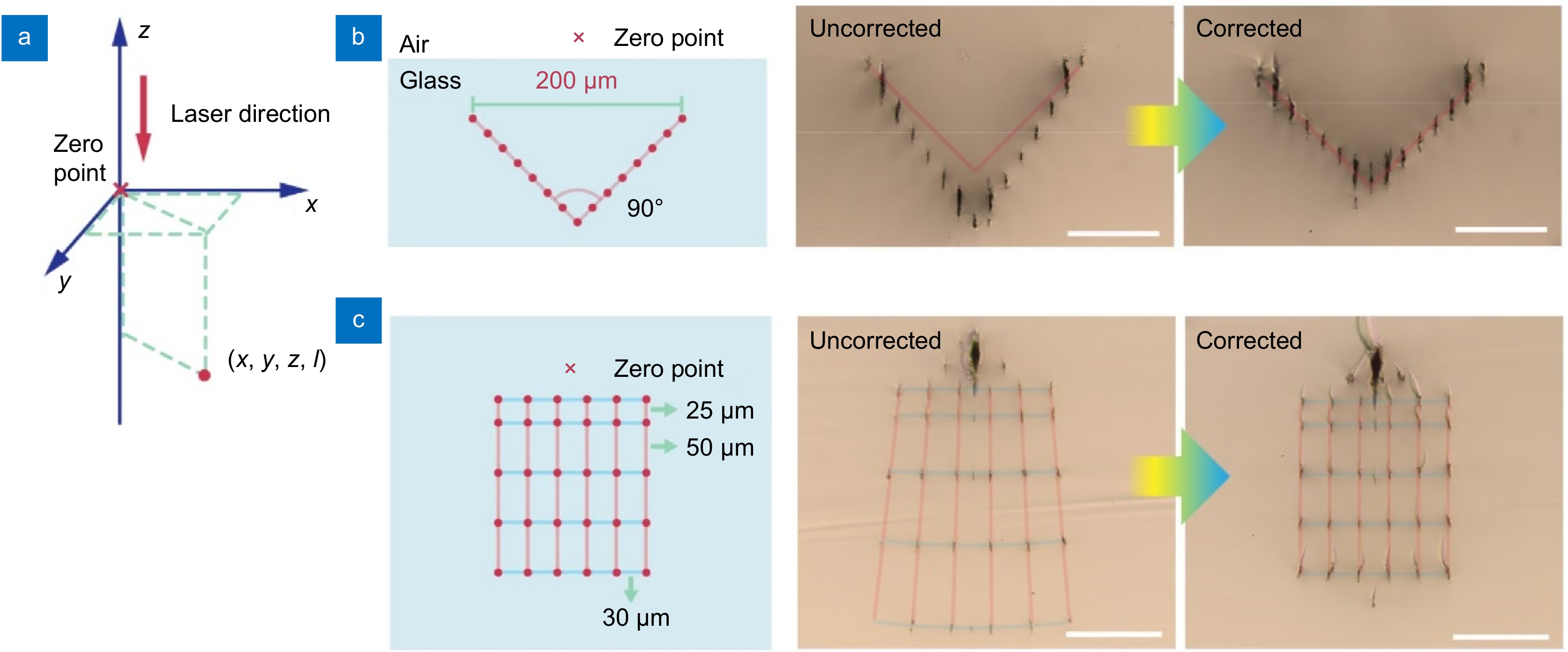
Correction of multi-focus modulation. (a) Illustration of single-spot coordinate. (b) Illustration of V-shaped design (left) and experimental results on fused silica produced by 20× objective without (middle) and with (right) refractive index correction. (c) Illustration of designed grid (left) with corresponding experimental results on fused silica produced by 50× objective without (middle) and with (right) complex correction. Scale bars: 100 μm.
-
Figure 3.
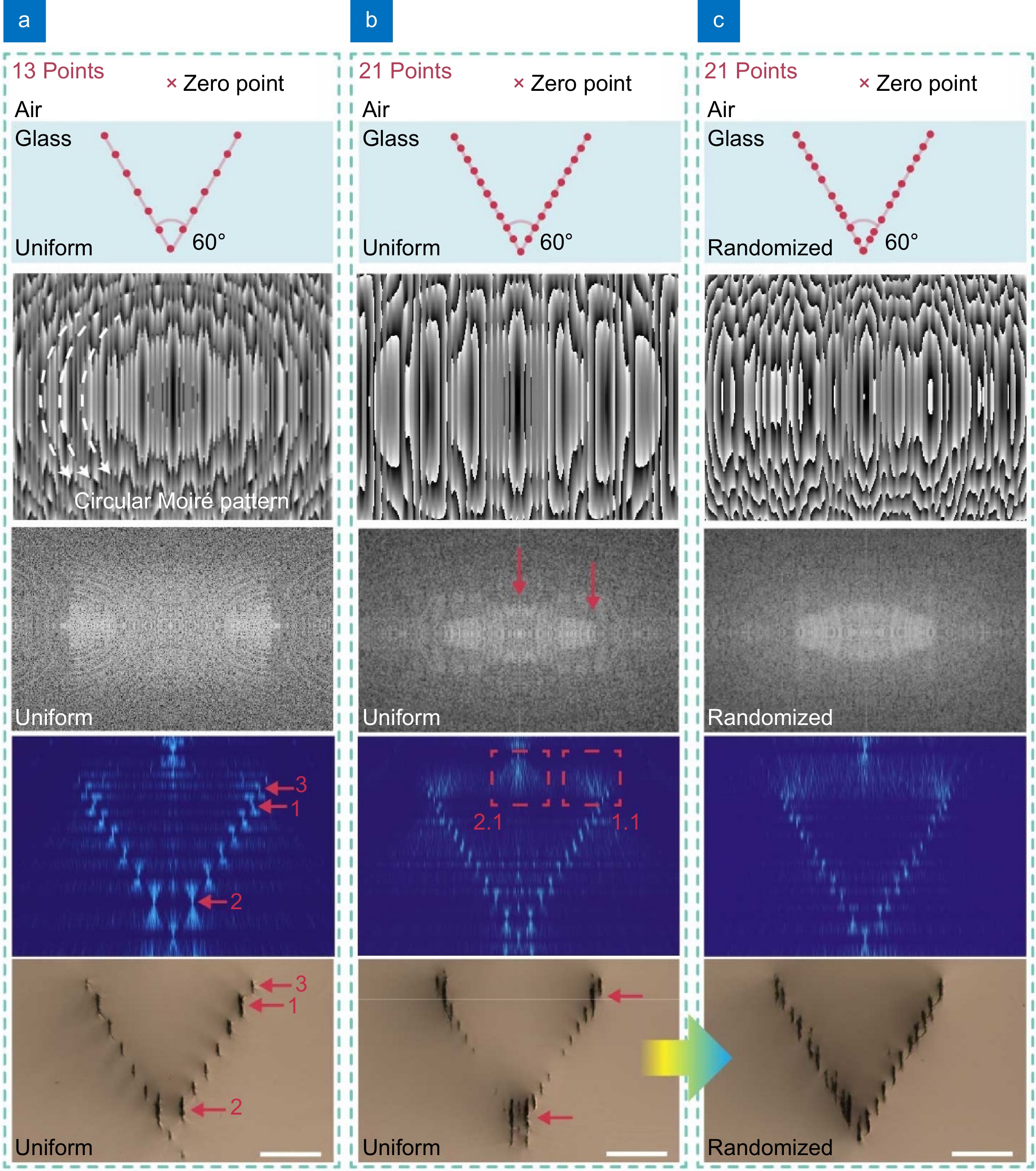
Uniformity improving of multi focus by randomization of their coordinates in fused silica. Illustration, phase diagram, fast Fourier transform images of phase diagrams showing circular Moiré patterns, light intensity field simulation, and bulk ablation of V-shape dot array with uniform multi foci of (a) 13 points , (b) 21 points , and (c) 21 points with randomized position. Scale bars: 100 μm.
-
Figure 4.
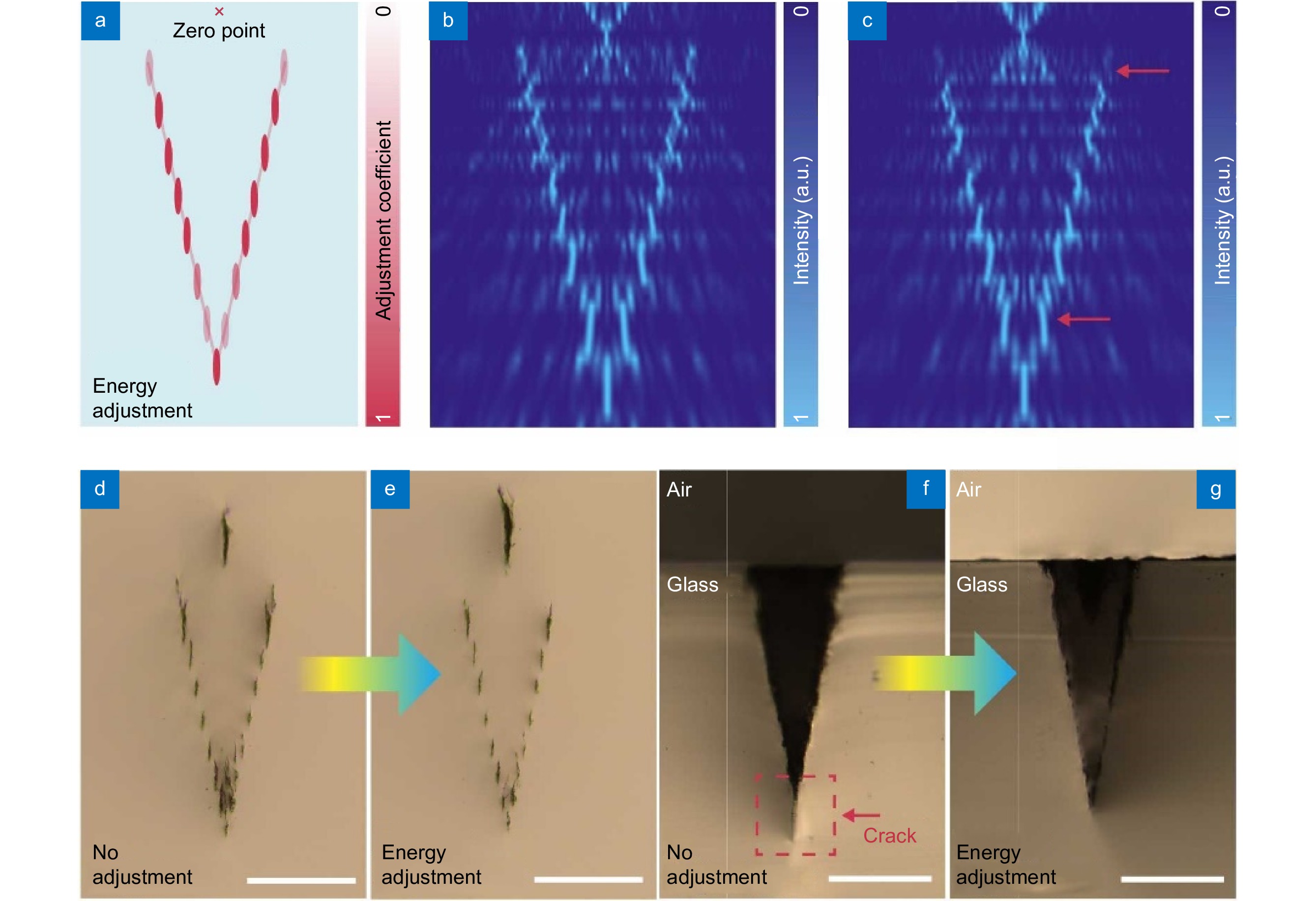
Point-by-point energy adjustment of dot array with high aspect ratio. (a) Illustration of selection of energy adjustment coefficient. Light intensity field simulation and experimental results on fused silica of 15-point array ablation or 33-point array without (b,d,f) and with energy adjustment (c,e,g). Scale bar: 100 μm.
-
Figure 5.
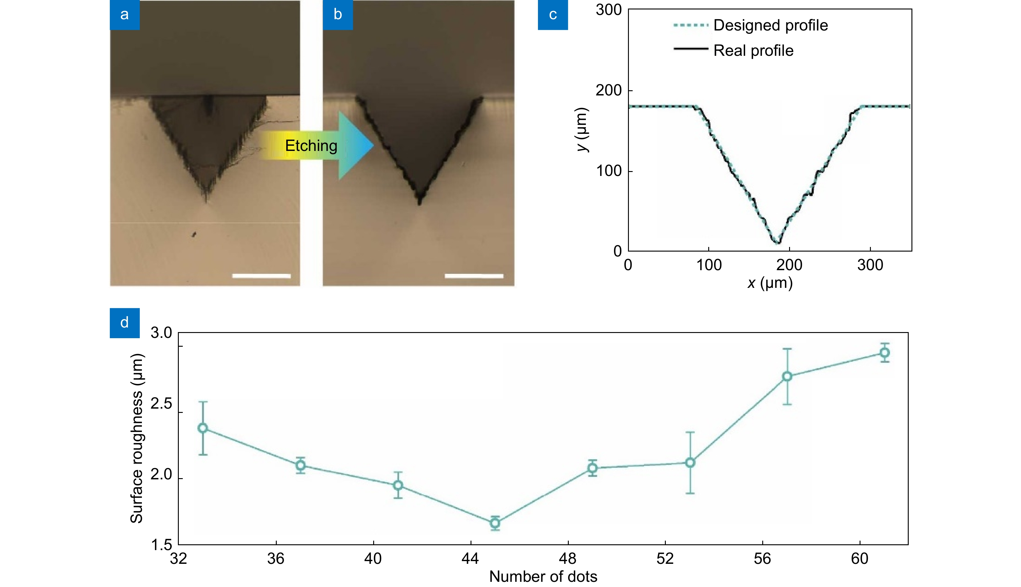
The profile and surface roughness of the V-shaped groove. (a) A V-shaped modified region processed by a multi-focus beam with 46 foci. (b) Etching result of V-shaped groove. (c) Designed profile and real profile of V-shaped groove. (d) Surface roughness of V-shaped grooves vary with the number of foci. Scale bars: 100 μm.
-
Figure 6.
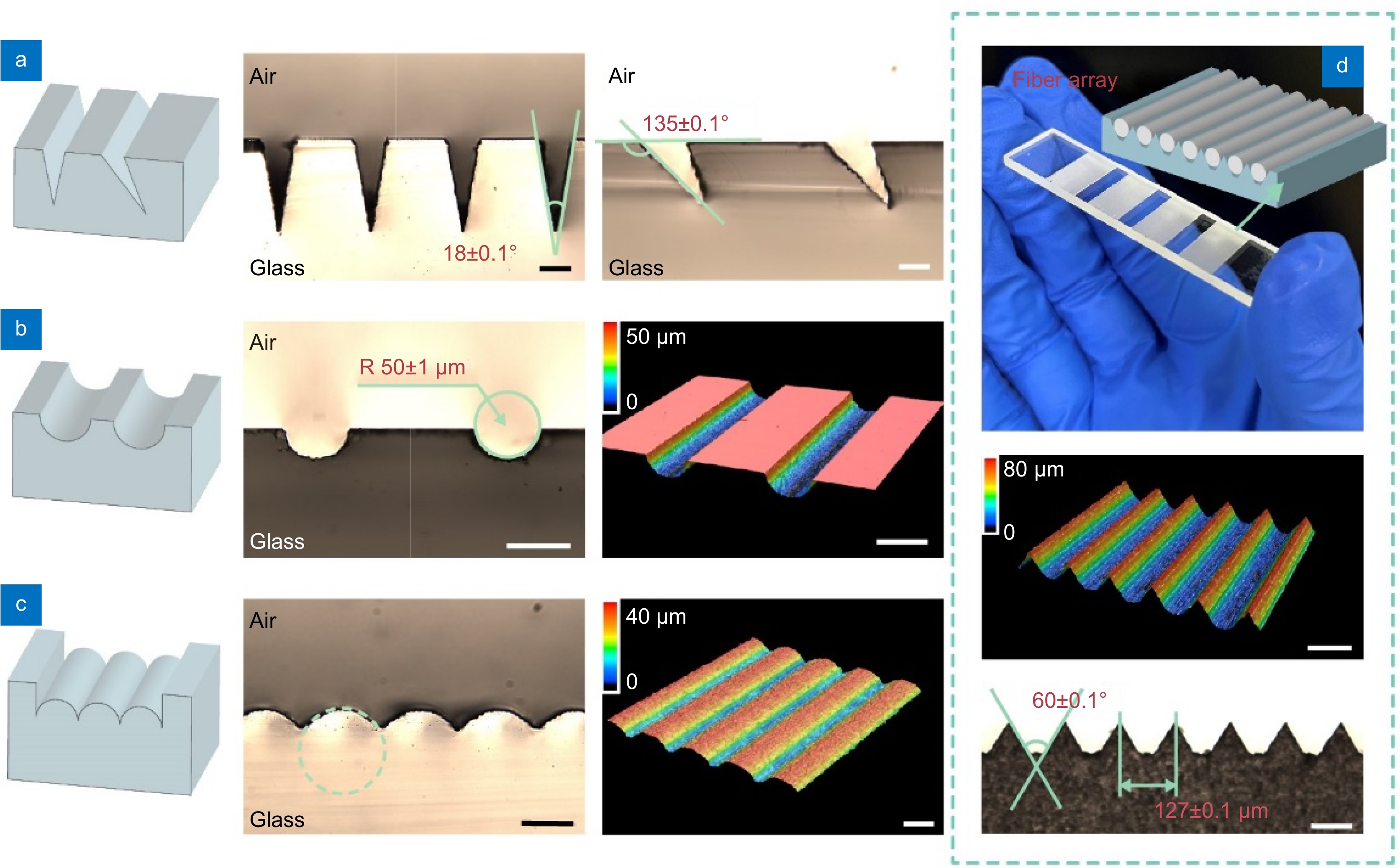
Diverse sectional profiles of glass grooves achieved through spatial multi-focus laser processing combined with chemical etching, along with their various applications. (a) Symmetric and asymmetric V-shaped grooves on fused silica. (b) Arc-shaped grooves on fused silica. (c) Cylinder arrays formed by continuous grooves on fused silica. (d) Trapezoid grooves on borosilicate glass used for optical fiber packaging. Scale bars: 100 μm.

 E-mail Alert
 RSS
RSS

 DownLoad:
