
 E-mail Alert
 RSS
RSS
| Citation: |
Fu JT, Leng CQ, Ma R et al. Photo-driven fin field-effect transistors. Opto-Electron Sci 3, 230046 (2024). doi: 10.29026/oes.2024.230046

|
-
Abstract
The integration between infrared detection and modern microelectronics offers unique opportunities for compact and high-resolution infrared imaging. However, silicon, the cornerstone of modern microelectronics, can only detect light within a limited wavelength range (< 1100 nm) due to its bandgap of 1.12 eV, which restricts its utility in the infrared detection realm. Herein, a photo-driven fin field-effect transistor is presented, which breaks the spectral response constraint of conventional silicon detectors while achieving sensitive infrared detection. This device comprises a fin-shaped silicon channel for charge transport and a lead sulfide film for infrared light harvesting. The lead sulfide film wraps the silicon channel to form a “three-dimensional” infrared-sensitive gate, enabling the photovoltage generated at the lead sulfide-silicon junction to effectively modulate the channel conductance. At room temperature, this device realizes a broadband photodetection from visible (635 nm) to short-wave infrared regions (2700 nm), surpassing the working range of the regular indium gallium arsenide and germanium detectors. Furthermore, it exhibits low equivalent noise powers of 3.2×10⁻¹² W·Hz−1/2 and 2.3×10⁻¹¹ W·Hz−1/2 under 1550 nm and 2700 nm illumination, respectively. These results highlight the significant potential of photo-driven fin field-effect transistors in advancing uncooled silicon-based infrared detection.-
Keywords:
- photodetection /
- silicon-on-insulator /
- lead sulfide /
- heterostructure /
- field-effect transistors
-

-
References
[1] Adinolfi V, Sargent EH. Photovoltage field-effect transistors. Nature 542, 324–327 (2017). doi: 10.1038/nature21050 [2] Yan HL, Li HN, Wang S et al. Overview of the LAMOST survey in the first decade. Innovation 3, 100224 (2022). [3] Li CH, Du W, Huang YX et al. Photonic synapses with ultralow energy consumption for artificial visual perception and brain storage. Opto-Electron Adv 5, 210069 (2022). doi: 10.29026/oea.2022.210069 [4] Zhang WL, Çakıroğlu O, Al-Enizi A et al. Solvent-free fabrication of broadband WS2 photodetectors on paper. Opto-Electron Adv 6, 220101 (2023). doi: 10.29026/oea.2023.220101 [5] Rogalski A. Infrared Detectors (CRC Press, Location, 2000). [6] Hu WD, Chen XS, Ye ZH et al. A hybrid surface passivation on HgCdTe long wave infrared detector with in-situ CdTe deposition and high-density hydrogen plasma modification. Appl Phys Lett 99, 091101 (2011). doi: 10.1063/1.3633103 [7] Hu WD, Ye ZH, Liao L et al. 128 × 128 long-wavelength/mid-wavelength two-color HgCdTe infrared focal plane array detector with ultralow spectral cross talk. Opt Lett 39, 5184–5187 (2014). doi: 10.1364/OL.39.005184 [8] Zeng LH, Han W, Ren XY et al. Uncooled mid-infrared sensing enabled by chip-integrated low-temperature-grown 2D PdTe2 dirac semimetal. Nano Lett 23, 8241–8248 (2023). doi: 10.1021/acs.nanolett.3c02396 [9] Rogalski A. Infrared detectors: status and trends. Prog Quantum Electron 27, 59–210 (2003). doi: 10.1016/S0079-6727(02)00024-1 [10] Wu PS, Ye L, Tong L et al. Van der Waals two-color infrared photodetector. Light Sci Appl 11, 6 (2022). doi: 10.1038/s41377-021-00694-4 [11] Zhou W, Zheng L, Ning ZJ et al. Silicon: quantum dot photovoltage triodes. Nat Commun 12, 6696 (2021). doi: 10.1038/s41467-021-27050-9 [12] Yan SQ, Zuo Y, Xiao SS et al. Graphene photodetector employing double slot structure with enhanced responsivity and large bandwidth. Opto-Electron Adv 5, 210159 (2022). doi: 10.29026/oea.2022.210159 [13] Xu KM, Xiao XB, Zhou WJ et al. Inverted Si: PbS colloidal quantum dot heterojunction-based infrared photodetector. ACS Appl Mater Interfaces 12, 15414–15421 (2020). doi: 10.1021/acsami.0c01744 [14] Masala S, Adinolfi V, Sun JP et al. The silicon: colloidal quantum dot heterojunction. Adv Mater 27, 7445–7450 (2015). doi: 10.1002/adma.201503212 [15] Michel J, Liu JF, Kimerling LC. High-performance Ge-on-Si photodetectors. Nat Photonics 4, 527–534 (2010). doi: 10.1038/nphoton.2010.157 [16] Shi YL, Wu ZM, Xiang ZH et al. Silicon-based PbS-CQDs infrared photodetector with high sensitivity and fast response. Nanotechnology 31, 485206 (2020). doi: 10.1088/1361-6528/abb105 [17] Shi YL, Wu ZM, Dong X et al. A silicon-based PbSe quantum dot near-infrared photodetector with spectral selectivity. Nanoscale 13, 12306–12313 (2021). doi: 10.1039/D1NR02037D [18] Chen PY, Wu ZM, Shi YL et al. High-performance silicon-based PbSe-CQDs infrared photodetector. J Mater Sci Mater Electron 32, 9452–9462 (2021). doi: 10.1007/s10854-021-05609-y [19] Ferain I, Colinge CA, Colinge JP. Multigate transistors as the future of classical metal–oxide–semiconductor field-effect transistors. Nature 479, 310–316 (2011). doi: 10.1038/nature10676 [20] Li MH, Zhou JJ, Tan LG et al. Multifunctional succinate additive for flexible perovskite solar cells with more than 23% power-conversion efficiency. Innovation 3, 100310 (2022). [21] Parmar JS, Sahu C. CMOS-compatible ex-situ incorporated junctionless enhancement-mode thin polysilicon film FET pH sensor. IEEE Trans Device Mater Reliab 21, 2–8 (2021). doi: 10.1109/TDMR.2020.3041190 [22] Sze SM, Ng KK. Physics of Semiconductor Devices 3rd ed (Wiley-Interscience, Hoboken, 2007). [23] Belin AM, Zolotarev VI, Nikiforov AY et al. 320 × 240 CMOS array for the spectral range of 3–5 μm based on PtSi photodiodes. Russ Microelectron 45, 474–477 (2016). doi: 10.1134/S1063739716070027 [24] Wu JH, Chang RS, Horng GJ. Microstructure, electrical, and optical properties of evaporated PtSi/p-Si(100) Schottky barriers as high quantum efficient infrared detectors. Thin Solid Films 466, 314–319 (2004). doi: 10.1016/j.tsf.2004.03.016 [25] Kay R, Bean R, Zanio K et al. HgCdTe photovoltaic detectors on Si substrates. Appl Phys Lett 51, 2211–2212 (1987). doi: 10.1063/1.98943 [26] Liu J, Liu PL, Chen DY et al. A near-infrared colloidal quantum dot imager with monolithically integrated readout circuitry. Nat Electron 5, 443–451 (2022). doi: 10.1038/s41928-022-00779-x [27] Fu JT, Nie CB, Sun FY et al. Photo-driven semimetal–semiconductor field-effect transistors. Adv Opt Mater 11, 2201983 (2023). doi: 10.1002/adom.202201983 [28] Vandamme EP, Vandamme LKJ. Critical discussion on unified 1/f noise models for MOSFETs. IEEE Trans Electron Devices 47, 2146–2152 (2000). doi: 10.1109/16.877177 [29] Almeida JM, Wisniowski P, Freitas PP. Low-frequency noise in MgO magnetic tunnel junctions: Hooge's parameter dependence on bias voltage. IEEE Trans Magn 44, 2569–2572 (2008). doi: 10.1109/TMAG.2008.2002604 [30] Cong H, Xue CL, Zheng J et al. Silicon based GeSn p-i-n photodetector for SWIR detection. IEEE Photonics J 8, 6804706 (2016). [31] Casalino M, Sassi U, Goykhman I et al. Vertically illuminated, resonant cavity enhanced, graphene-silicon schottky photodetectors. ACS Nano 11, 10955–10963 (2017). doi: 10.1021/acsnano.7b04792 [32] Goykhman I, Sassi U, Desiatov B et al. On-chip integrated, silicon-graphene plasmonic schottky photodetector with high responsivity and avalanche photogain. Nano Lett 16, 3005–3013 (2016). doi: 10.1021/acs.nanolett.5b05216 [33] Casalino M, Russo R, Russo C et al. Free-space schottky graphene/silicon photodetectors operating at 2 μm. ACS Photonics 5, 4577–4585 (2018). doi: 10.1021/acsphotonics.8b01037 [34] Tanzid M, Ahmadivand A, Zhang RM et al. Combining plasmonic hot carrier generation with free carrier absorption for high-performance near-infrared silicon-based photodetection. ACS Photonics 5, 3472–3477 (2018). doi: 10.1021/acsphotonics.8b00623 [35] Hu F, Dai XY, Zhou ZQ et al. Black silicon Schottky photodetector in sub-bandgap near-infrared regime. Opt Express 27, 3161–3168 (2019). doi: 10.1364/OE.27.003161 [36] Huang S, Wu Q, Jia ZX et al. Black silicon photodetector with excellent comprehensive properties by rapid thermal annealing and hydrogenated surface passivation. Adv Opt Mater 8, 1901808 (2020). doi: 10.1002/adom.201901808 [37] Zhao XN, Lin K, Zhao B et al. Broadband MSM photodetector based on S-doped black silicon fabricated by femtosecond laser. Appl Surf Sci 619, 156624 (2023). doi: 10.1016/j.apsusc.2023.156624 [38] Zhang YB, Loh JYY, Kherani NP. Facilely achieved self-biased black silicon heterojunction photodiode with broadband quantum efficiency approaching 100%. Adv Sci (Weinh) 9, 2203234 (2022). doi: 10.1002/advs.202203234 [39] Wang M, García-Hemme E, Berencén Y et al. Silicon-based intermediate-band infrared photodetector realized by Te hyperdoping. Adv Opt Mater 9, 2001546 (2021). doi: 10.1002/adom.202001546 [40] Wang L, Jie JS, Shao ZB et al. MoS2/Si heterojunction with vertically standing layered structure for ultrafast, high-detectivity, self-driven visible-near infrared photodetectors. Adv Funct Mater 25, 2910–2919 (2015). doi: 10.1002/adfm.201500216 [41] An XH, Liu FZ, Jung YJ et al. Tunable graphene-silicon heterojunctions for ultrasensitive photodetection. Nano Lett 13, 909–916 (2013). doi: 10.1021/nl303682j [42] Huang K, Yan YC, Li K et al. High and fast response of a graphene-silicon photodetector coupled with 2D fractal platinum nanoparticles. Adv Opt Mater 6, 1700793 (2018). doi: 10.1002/adom.201700793 [43] You S, Zhang L, Yu YQ et al. Nanoscale AgInTe2/Si truncated quasitetrahedrons for heterostructured photodetectors. ACS Appl Nano Mater 4, 5785–5795 (2021). doi: 10.1021/acsanm.1c00598 -
Supplementary Information
Supplementary information for Photo-driven fin field-effect transistor 
-
Access History
Figures(4)
Article Metrics

Export File
Citation
Fu JT, Leng CQ, Ma R et al. Photo-driven fin field-effect transistors. Opto-Electron Sci 3, 230046 (2024). doi: 10.29026/oes.2024.230046
Format
Content
 DownLoad:
-
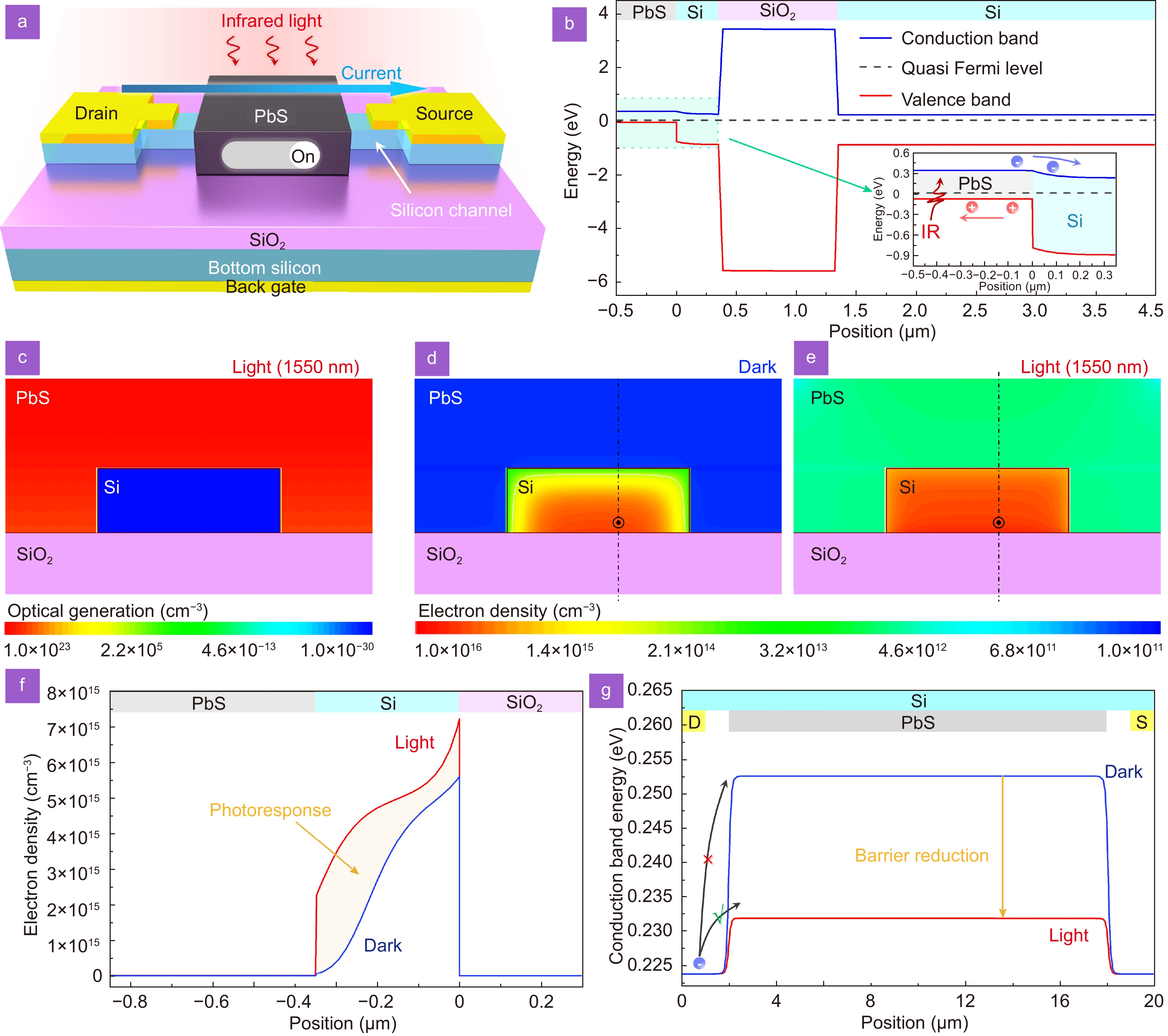
Figure 1.
Device structure and working mechanism of the photo-FinFET. (a) A schematic illustration of the PbS-Si photo-FinFET. Infrared light “switches on” the PbS gate, allowing current to flow through the Si channel. (b) Energy band simulation results along the vertical direction of the Si channel. Inset: an enlarged view of the light green box, in which a schematic diagram of the dynamic process of photogenerated carriers under infrared illumination is depicted. (c) Simulated optical generation in the photo-FinFET under excitation by 1550 nm light. (d, e) Simulated electron (majority carriers) density in the photo-FinFET under darkness and 1550 nm illumination, respectively. (f) Electron density extracted along the dash-dotted lines in (d) and (e). (g) Conduction band energy extracted along the Si channel, i.e., the direction indicated by circles and dots in (d) and (e).
-
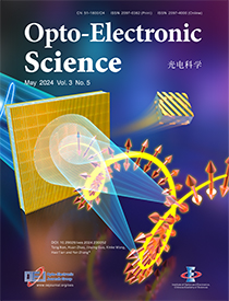
Figure 2.
Visible photoresponse and modulation characteristic of the photo-FinFET. (a) Transfer characteristic curves of the photo-FinFET under 635 nm illumination with varying power densities. (b) Top panel: transfer characteristic curve of the photo-FinFET in the dark state. Bottom panel: schematic diagrams of the carrier dynamics process in the channel of the photo-FinFET when it is in the depletion region and working region, respectively. (c) Output characteristic curves of the photo-FinFET under 635 nm illumination with different power densities. (d) Photocurrent and responsivity as a function of light power density.
-
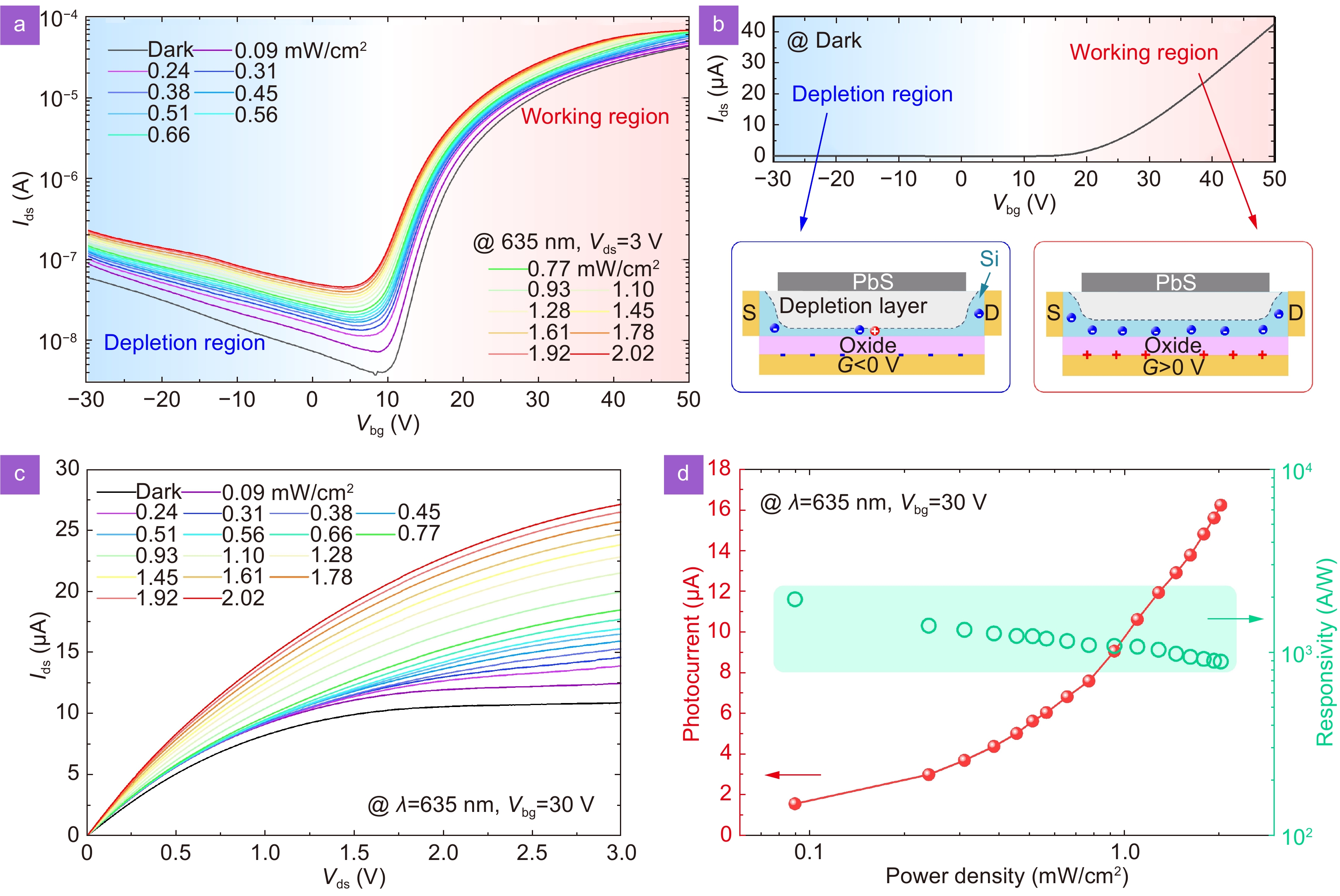
Figure 3.
Infrared phototresponse of the photo-FinFET. (a, b) I-T curves of the photo-FinFET in response to 1550 nm and 2700 nm illumination under different Vbg. The power densities of the 1550 nm and 2700 nm illumination are 603.13 mW/cm2 and 87.04 mW/cm2, respectively. (c, d) Responsivity of the photo-FinFET as a function of the light power density under different Vbg. The wavelengths of the light sources are 1550 nm and 2700 nm, respectively.
-
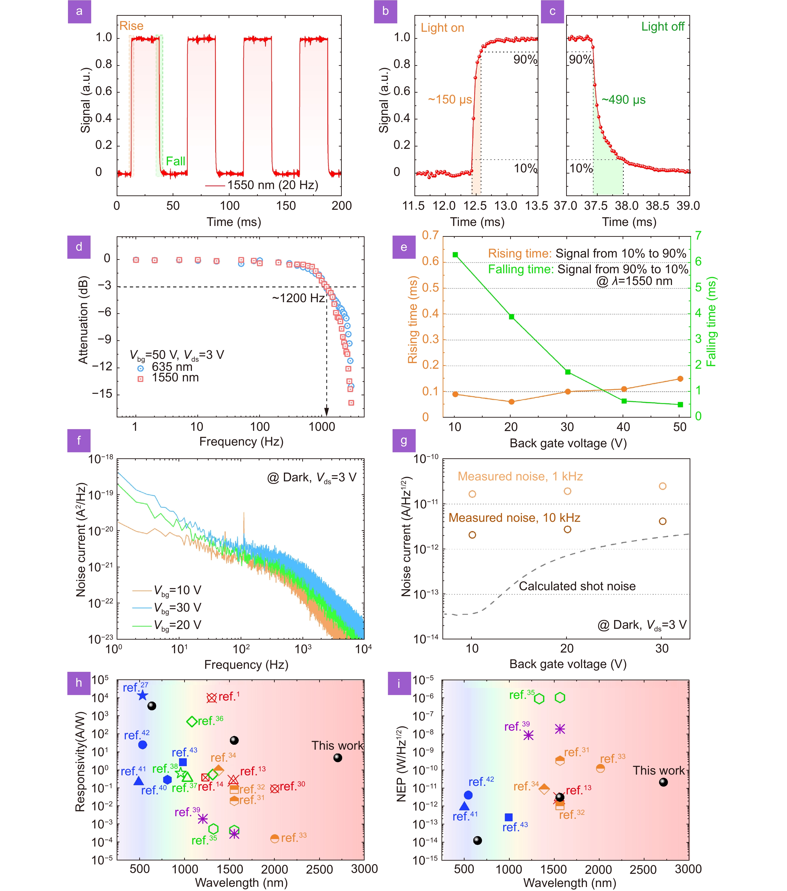
Figure 4.
Response speed, noise and performance summary of the photo-FinFET. (a) Output signal of the photo-FinFET as a function of time under 1550 nm illumination. (b, c) Enlarged views of the rising and falling edges (indicated by the shaded boxed regions in (a)). (d) 3 dB bandwidth measurement results of the photo-FinFET under 635 nm and 1550 nm illumination. (e) Rising and falling times of the photo-FinFET at different Vbg. (f) Noise current of the photo-FinFET at different Vbg. (g) Measured noise current and calculated shot noise of the photo-FinFET. The calculation formula of shot noise is 2qIdark, where q is the elemental charge and Idark is the dark current. (h, i) Performance comparison of the photo-FinFET with previously reported Si-based photodetectors. The responsivity and NEP of the photo-FinFET presented in (h) and (i) are measured at Vbg = 50 V and Vbg = 30 V, respectively. These previously reported Si-based photodetectors are based on different strategies to enable infrared photodetection including, integrating infrared-absorbing materials (red icons), utilizing internal photoemission effect (orange icons), manufacturing black Si (green icons), exploiting intrinsic light absorption of Si (blue icons), and hyper-doping Si (purple icons). Parameters of the photo-FinFET are indicated by black icons.


