
 E-mail Alert
 RSS
RSS
| Citation: |
Dong B, Zhang J, Wang D W, et al. Femtosecond laser micromachining optical devices[J]. Opto-Electron Eng, 2023, 50(3): 220073. doi: 10.12086/oee.2023.220073

|
Femtosecond laser micromachining optical devices
-
Abstract
Miniaturization, integration, and flexible deformation are the future development trends of optical devices. Meanwhile, optical systems based on integrated micro-optical devices stand out for their low power consumption, fast response, and high information storage capacity. However, current high-precision micro/nano processing methods, such as FIB (Focused Ion Beam) and semiconductor lithography, are far too complex and in lack of flexibility. Femtosecond laser, as a non-contact, high-precision, high-intensity tool for "cold" processing, is particularly favored in micro/nano processing. This review first elucidated the background and mechanism of femtosecond laser micromachining used in optical device. After that, we discussed a number of methods employed to improve the resolution of femtosecond micromachining. Then we listed various advanced processing means based on femtosecond laser and systematically summarized recent representative research developments of femtosecond laser micromachining used in microlens, gratings, optical waveguides, and photonic crystals. Finally, we concluded the challenges and the directions for further development of femtosecond laser machining in the field of micro-optical devices.-
Keywords:
- femtosecond laser /
- high-precision /
- micro/nano structure /
- optical device
-

-
References
[1] Maruo S, Nakamura O, Kawata S. Three-dimensional microfabrication with two-photon-absorbed photopolymerization[J]. Opt Lett, 1997, 22(2): 132−134. doi: 10.1364/OL.22.000132 [2] 杨建军. 飞秒激光超精细“冷”加工技术及其应用(续)[J]. 激光与光电子学进展, 2004, 41(4): 39−47. Yang J J. Femtosecond laser “cold” micro-machining and its advanced applications (Ⅱ)[J]. Laser Optoelectron Prog, 2004, 41(4): 39−47. [3] Cao Y Y, Gan Z S, Jia B H, et al. High-photosensitive resin for super-resolution direct-laser-writing based on photoinhibited polymerization[J]. Opt Express, 2011, 19(20): 19486−19494. doi: 10.1364/OE.19.019486 [4] Gan Z S, Cao Y Y, Evans R A, et al. Three-dimensional deep sub-diffraction optical beam lithography with 9 nm feature size[J]. Nat Commun, 2013, 4(1): 2061. doi: 10.1038/ncomms3061 [5] Chichkov B N, Momma C, Nolte S, et al. Femtosecond, picosecond and nanosecond laser ablation of solids[J]. Appl Phys A, 1996, 63(2): 109−115. doi: 10.1007/BF01567637 [6] Sugioka K, Cheng Y. Femtosecond laser three-dimensional micro-and nanofabrication[J]. Appl Phys Rev, 2014, 1(4): 041303. doi: 10.1063/1.4904320 [7] Davis K M, Miura K, Sugimoto N, et al. Writing waveguides in glass with a femtosecond laser[J]. Opt Lett, 1996, 21(21): 1729−1731. doi: 10.1364/OL.21.001729 [8] Glezer E N, Milosavljevic M, Huang L, et al. Three-dimensional optical storage inside transparent materials[J]. Opt Lett, 1996, 21(24): 2023−2025. doi: 10.1364/OL.21.002023 [9] Miyamoto I, Horn A, Gottmann J, et al. Fusion welding of glass using femtosecond laser pulses with high-repetition rates[J]. J Laser Micro Nanoen, 2007, 2(1): 57−63. doi: 10.2961/jlmn.2007.01.0011 [10] Cheng Y, Sugioka K, Midorikawa K, et al. Three-dimensional micro-optical components embedded in photosensitive glass by a femtosecond laser[J]. Opt Lett, 2003, 28(13): 1144−1146. doi: 10.1364/OL.28.001144 [11] Cheng Y, Sugioka K, Midorikawa K. Microfluidic laser embedded in glass by three-dimensional femtosecond laser microprocessing[J]. Opt Lett, 2004, 29(17): 2007−2009. doi: 10.1364/OL.29.002007 [12] Liu H L, Jia Y C, de Aldana J R V, et al. Femtosecond laser inscribed cladding waveguides in Nd: YAG ceramics: fabrication, fluorescence imaging and laser performance[J]. Opt Express, 2012, 20(17): 18620−18629. doi: 10.1364/OE.20.018620 [13] Mizeikis V, Purlys V, Buividas R, et al. Realization of structural color by direct laser write technique in photoresist[J]. J Laser Micro Nanoen, 2014, 9(1): 42−45. doi: 10.2961/jlmn.2014.01.0009 [14] Cheng Y, Sugioka K, Midorikawa K, et al. Control of the cross-sectional shape of a hollow microchannel embedded in photostructurable glass by use of a femtosecond laser[J]. Opt Lett, 2003, 28(1): 55−57. doi: 10.1364/OL.28.000055 [15] Osellame R, Taccheo S, Marangoni M, et al. Femtosecond writing of active optical waveguides with astigmatically shaped beams[J]. J Opt Soc Am B, 2003, 20(7): 1559−1567. doi: 10.1364/JOSAB.20.001559 [16] He F, Xu H, Cheng Y, et al. Fabrication of microfluidic channels with a circular cross section using spatiotemporally focused femtosecond laser pulses[J]. Opt Lett, 2010, 35(7): 1106−1108. doi: 10.1364/OL.35.001106 [17] Liew W L A, Zhang Y L. Laser-based fabrication of 3D hydrogel constructs using bessel beams[J]. Bioprinting, 2018, 9: 44−51. doi: 10.1016/j.bprint.2018.02.004 [18] Wang Z, Jiang L, Li X W, et al. High-throughput microchannel fabrication in fused silica by temporally shaped femtosecond laser Bessel-beam-assisted chemical etching[J]. Opt Lett, 2018, 43(1): 98−101. doi: 10.1364/OL.43.000098 [19] Kawata S, Sun H B, Tanaka T, et al. Finer features for functional microdevices[J]. Nature, 2001, 412(6848): 697−698. doi: 10.1038/35089130 [20] Liao C Z, Anderson W, Antaw F, et al. Two-photon nanolithography of tailored hollow three-dimensional microdevices for biosystems[J]. ACS Omega, 2019, 4(1): 1401−1409. doi: 10.1021/acsomega.8b03164 [21] Cai Z, Qi X B, Pan D, et al. Dynamic Airy imaging through high-efficiency broadband phase microelements by femtosecond laser direct writing[J]. Photonics Res, 2020, 8(6): 875−883. doi: 10.1364/PRJ.387495 [22] Xu L Q, Wang C W, Qi X B, et al. Femtosecond laser direct writing continuous phase vortex gratings with proportionally distributed diffraction energy[J]. Appl Phys Lett, 2021, 119(13): 131101. doi: 10.1063/5.0061590 [23] Liu S L, Ni J C, Zhang C, et al. Tailoring optical vortical dichroism with stereometamaterials[J]. Laser Photonics Rev, 2022, 16(2): 2100518. doi: 10.1002/lpor.202100518 [24] Ni J C, Liu S L, Hu G W, et al. Giant helical dichroism of single chiral nanostructures with photonic orbital angular momentum[J]. ACS Nano, 2021, 15(2): 2893−2900. doi: 10.1021/acsnano.0c08941 [25] Ma Z C, Hu X Y, Zhang Y L, et al. Smart compound eyes enable tunable imaging[J]. Adv Funct Mater, 2019, 29(38): 1903340. doi: 10.1002/adfm.201903340 [26] Hu Y L, Wang Z Y, Jin D D, et al. Botanical‐inspired 4D printing of hydrogel at the microscale[J]. Adv Funct Mater, 2020, 30(4): 1907377. doi: 10.1002/adfm.201907377 [27] Zhang Y L, Tian Y, Wang H, et al. Dual-3D femtosecond laser nanofabrication enables dynamic actuation[J]. ACS Nano, 2019, 13(4): 4041−4048. doi: 10.1021/acsnano.8b08200 [28] Lv C, Sun X C, Xia H, et al. Humidity-responsive actuation of programmable hydrogel microstructures based on 3D printing[J]. Sensor Actuat B Chem, 2018, 259: 736−744. doi: 10.1016/j.snb.2017.12.053 [29] Xin C, Jin D D, Hu Y L, et al. Environmentally adaptive shape-morphing microrobots for localized cancer cell treatment[J]. ACS Nano, 2021, 15(11): 18048−18059. doi: 10.1021/acsnano.1c06651 [30] Chen Q Y, Lv P Y, Huang T Y, et al. Encoding smart microjoints for microcrawlers with enhanced locomotion[J]. Adv Intell Syst, 2020, 2(3): 1900128. doi: 10.1002/aisy.201900128 [31] Jin D D, Chen Q Y, Huang T Y, et al. Four-dimensional direct laser writing of reconfigurable compound micromachines[J]. Mater Today, 2020, 32: 19−25. doi: 10.1016/j.mattod.2019.06.002 [32] Huang T Y, Huang H W, Jin D D, et al. Four-dimensional micro-building blocks[J]. Sci Adv, 2020, 6(3): eaav8219. doi: 10.1126/sciadv.aav8219 [33] Huang Z C, Chen C, Wang X H, et al. Light-driven locomotion of underwater bubbles on ultrarobust paraffin-impregnated laser-ablated Fe3O4-doped slippery surfaces[J]. ACS Appl Mater Interfaces, 2021, 13(7): 9272−9280. doi: 10.1021/acsami.0c22717 [34] Chen C, Zhou L L, Shi L A, et al. Ultralow-voltage-driven smart control of diverse drop’s anisotropic sliding by in situ switching joule heat on paraffin-infused microgrooved slippery surface[J]. ACS Appl Mater Interfaces, 2020, 12(1): 1895−1904. doi: 10.1021/acsami.9b17936 [35] Chen C, Huang Z C, Jiao Y L, et al. In situ reversible control between sliding and pinning for diverse liquids under ultra-low voltage[J]. ACS Nano, 2019, 13(5): 5742−5752. doi: 10.1021/acsnano.9b01180 [36] Chen C, Shi L A, Huang Z C, et al. Microhole‐arrayed PDMS with controllable wettability gradient by one‐step femtosecond laser drilling for ultrafast underwater bubble unidirectional self‐transport[J]. Adv Mater Interfaces, 2019, 6(12): 1900297. doi: 10.1002/admi.201900297 [37] Jiang S J, Hu Y L, Wu H, et al. Multifunctional Janus Microplates arrays actuated by magnetic fields for water/light switches and bio‐inspired assimilatory coloration[J]. Adv Mater, 2019, 31(15): 1807507. doi: 10.1002/adma.201807507 [38] Jiang S J, Hu Y L, Wu H, et al. Three-dimensional multifunctional magnetically responsive liquid manipulator fabricated by femtosecond laser writing and soft transfer[J]. Nano Lett, 2020, 20(10): 7519−7529. doi: 10.1021/acs.nanolett.0c02997 [39] Liu J K, Jia X, Wu W S, et al. Ultrafast imaging on the formation of periodic ripples on a Si surface with a prefabricated nanogroove induced by a single femtosecond laser pulse[J]. Opt Express, 2018, 26(5): 6302−6315. doi: 10.1364/OE.26.006302 [40] Buividas R, Rekštytė S, Malinauskas M, et al. Nano-groove and 3D fabrication by controlled avalanche using femtosecond laser pulses[J]. Opt Mater Express, 2013, 3(10): 1674−1686. doi: 10.1364/OME.3.001674 [41] Li Z Z, Wang L, Fan H, et al. O-FIB: far-field-induced near-field breakdown for direct nanowriting in an atmospheric environment[J]. Light Sci Appl, 2020, 9(1): 41. doi: 10.1038/s41377-020-0275-2 [42] Lin J T, Yu S J, Ma Y G, et al. On-chip three-dimensional high-Q microcavities fabricated by femtosecond laser direct writing[J]. Opt Express, 2012, 20(9): 10212−10217. doi: 10.1364/OE.20.010212 [43] Xu H L, Sun H B. Femtosecond laser 3D fabrication of whispering-gallery-mode microcavities[J]. Sci China Phys Mech Astron, 2015, 58(11): 114202. doi: 10.1007/s11433-015-5720-5 [44] Wu H, Zhang L R, Jiang S J, et al. Ultrathin and high-stress-resolution liquid-metal-based pressure sensors with simple device structures[J]. ACS Appl Mater Interfaces, 2020, 12(49): 55390−55398. doi: 10.1021/acsami.0c16250 [45] Huang J, Jiang L, Li X W, et al. Fabrication of highly homogeneous and controllable nanogratings on silicon via chemical etching-assisted femtosecond laser modification[J]. Nanophotonics, 2019, 8(5): 869−878. doi: 10.1515/nanoph-2019-0056 [46] Liu Y, Li S Y, Niu S C, et al. Bio-inspired micro-nano structured surface with structural color and anisotropic wettability on Cu substrate[J]. Appl Surf Sci, 2016, 379: 230−237. doi: 10.1016/j.apsusc.2016.03.234 [47] Kuroiwa Y, Takeshima N, Narita Y, et al. Arbitrary micropatterning method in femtosecond laser microprocessing using diffractive optical elements[J]. Opt Express, 2004, 12(9): 1908−1915. doi: 10.1364/OPEX.12.001908 [48] Torres-Peiró S, González-Ausejo J, Mendoza-Yero O, et al. Parallel laser micromachining based on diffractive optical elements with dispersion compensated femtosecond pulses[J]. Opt Express, 2013, 21(26): 31830−31836. doi: 10.1364/OE.21.031830 [49] Maibohm C, Silvestre O F, Borme J, et al. Multi-beam two-photon polymerization for fast large area 3D periodic structure fabrication for bioapplications[J]. Sci Rep, 2020, 10(1): 8740. doi: 10.1038/s41598-020-64955-9 [50] Wang X D, Yu H B, Li P W, et al. Femtosecond laser-based processing methods and their applications in optical device manufacturing: a review[J]. Opt Laser Technol, 2021, 135: 106687. doi: 10.1016/j.optlastec.2020.106687 [51] Gu C L, Zhang D P, Chang Y N, et al. Digital micromirror device-based ultrafast pulse shaping for femtosecond laser[J]. Opt Lett, 2015, 40(12): 2870−2873. doi: 10.1364/OL.40.002870 [52] Cheng J Y, Gu C L, Zhang D P, et al. High-speed femtosecond laser beam shaping based on binary holography using a digital micromirror device[J]. Opt Lett, 2015, 40(21): 4875−4878. doi: 10.1364/OL.40.004875 [53] Guo Y M, Wang Y, Hu Q L, et al. High-resolution femtosecond laser beam shaping via digital holography[J]. Opt Lett, 2019, 44(4): 987−990. doi: 10.1364/OL.44.000987 [54] Mills B, Heath D J, Feinaeugle M, et al. Laser ablation via programmable image projection for submicron dimension machining in diamond[J]. J Laser Appl, 2014, 26(4): 041501. doi: 10.2351/1.4893749 [55] Gu C L, Zhang D P, Wang D E, et al. Parallel femtosecond laser light sheet micro-manufacturing based on temporal focusing[J]. Precis Eng, 2017, 50: 198−203. doi: 10.1016/j.precisioneng.2017.05.006 [56] Wang D E, Wen C Y, Chang Y N, et al. Ultrafast laser-enabled 3D metal printing: a solution to fabricate arbitrary submicron metal structures[J]. Precis Eng, 2018, 52: 106−111. doi: 10.1016/j.precisioneng.2017.11.015 [57] Saha S K, Wang D E, Nguyen V H, et al. Scalable submicrometer additive manufacturing[J]. Science, 2019, 366(6461): 105−109. doi: 10.1126/science.aax8760 [58] Hasegawa S, Hayasaki Y, Nishida N. Holographic femtosecond laser processing with multiplexed phase Fresnel lenses[J]. Opt Lett, 2006, 31(11): 1705−1707. doi: 10.1364/OL.31.001705 [59] Zhang C C, Hu Y L, Du W Q, et al. Optimized holographic femtosecond laser patterning method towards rapid integration of high-quality functional devices in microchannels[J]. Sci Rep, 2016, 6: 33281. doi: 10.1038/srep33281 [60] Wang D, Xiao D, Li N N, et al. Holographic display system based on effective area expansion of SLM[J]. IEEE Photonics J, 2019, 11(6): 7001312. [61] Blinder D, Schelkens P. Phase added sub-stereograms for accelerating computer generated holography[J]. Opt Express, 2020, 28(11): 16924−16934. doi: 10.1364/OE.388881 [62] Xu B, Du W Q, Li J W, et al. High efficiency integration of three-dimensional functional microdevices inside a microfluidic chip by using femtosecond laser multifoci parallel microfabrication[J]. Sci Rep, 2016, 6: 19989. doi: 10.1038/srep19989 [63] Ni J C, Wang C W, Zhang C C, et al. Three-dimensional chiral microstructures fabricated by structured optical vortices in isotropic material[J]. Light Sci Appl, 2017, 6(7): e17011. doi: 10.1038/lsa.2017.11 [64] Pan D, Liu S L, Li J W, et al. Rapid fabrication of 3D chiral microstructures by single exposure of interfered femtosecond vortex beams and capillary‐force‐assisted self‐assembly[J]. Adv Funct Mater, 2022, 32(4): 2106917. doi: 10.1002/adfm.202106917 [65] Xin C, Yang L, Li J W, et al. Conical hollow microhelices with superior swimming capabilities for targeted cargo delivery[J]. Adv Mater, 2019, 31(25): 1808226. doi: 10.1002/adma.201808226 [66] Wang C W, Yang L, Hu Y L, et al. Femtosecond mathieu beams for rapid controllable fabrication of complex microcages and application in trapping microobjects[J]. ACS Nano, 2019, 13(4): 4667−4676. doi: 10.1021/acsnano.9b00893 [67] Xu B, Ji S Y, Pan D, et al. Hybrid femtosecond laser fabrication of a size-tunable microtrap chip with a high-trapping retention rate[J]. Opt Lett, 2020, 45(5): 1071−1074. doi: 10.1364/OL.386095 [68] Pan D, Cai Z, Ji S Y, et al. Microtubes with complex cross section fabricated by C-shaped bessel laser beam for mimicking stomata that opens and closes rapidly[J]. ACS Appl Mater Interfaces, 2018, 10(42): 36369−36376. doi: 10.1021/acsami.8b11173 [69] Ji S Y, Yang L, Zhang C C, et al. High-aspect-ratio microtubes with variable diameter and uniform wall thickness by compressing Bessel hologram phase depth[J]. Opt Lett, 2018, 43(15): 3514−3517. doi: 10.1364/OL.43.003514 [70] Li R, Jin D D, Pan D, et al. Stimuli-responsive actuator fabricated by dynamic asymmetric femtosecond bessel beam for in situ particle and cell manipulation[J]. ACS Nano, 2020, 14(5): 5233−5242. doi: 10.1021/acsnano.0c00381 [71] Yan L Y, Yang D, Gong Q H, et al. Rapid fabrication of continuous surface Fresnel microlens array by femtosecond laser focal field engineering[J]. Micromachines, 2020, 11(2): 112. doi: 10.3390/mi11020112 [72] Yang D, Liu L P, Gong Q H, et al. Rapid two‐photon polymerization of an arbitrary 3D microstructure with 3D focal field engineering[J]. Macromol Rapid Commun, 2019, 40(8): 1900041. doi: 10.1002/marc.201900041 [73] Chu W, Tan Y X, Wang P, et al. Centimeter‐height 3D printing with femtosecond laser two‐photon polymerization[J]. Adv Mater Technol, 2018, 3(5): 1700396. doi: 10.1002/admt.201700396 [74] Wang P, Chu W, Li W B, et al. Three-dimensional laser printing of macro-scale glass objects at a micro-scale resolution[J]. Micromachines, 2019, 10(9): 565. doi: 10.3390/mi10090565 [75] Uesugi Y, Fukushima R, Saitoh K, et al. Creating electron phase holograms using femtosecond laser interference processing[J]. Opt Express, 2019, 27(15): 20958−20964. doi: 10.1364/OE.27.020958 [76] Li B H, Jiang L, Li X W, et al. Flexible gray‐scale surface patterning through spatiotemporal‐interference‐based femtosecond laser shaping[J]. Adv Opt Mater, 2018, 6(24): 1801021. doi: 10.1002/adom.201801021 [77] Wang M M, Guo Q T, Wang S M, et al. Interference femtosecond laser stamping of micro-grating structures and time-resolved observation of its dynamics[J]. Opt Express, 2020, 28(12): 18376−18386. doi: 10.1364/OE.390012 [78] Wu H, Jiao Y L, Zhang C C, et al. Large area metal micro-/nano-groove arrays with both structural color and anisotropic wetting fabricated by one-step focused laser interference lithography[J]. Nanoscale, 2019, 11(11): 4803−4810. doi: 10.1039/C8NR09747J [79] Nakata Y, Murakawa K, Miyanaga N, et al. Local melting of gold thin films by femtosecond laser-interference processing to generate nanoparticles on a source target[J]. Nanomaterials, 2018, 8(7): 477. doi: 10.3390/nano8070477 [80] Shrestha S, Overvig A C, Lu M, et al. Broadband achromatic dielectric metalenses[J]. Light Sci Appl, 2018, 7: 85. doi: 10.1038/s41377-018-0078-x [81] Nagelberg S, Zarzar L D, Nicolas N, et al. Reconfigurable and responsive droplet-based compound micro-lenses[J]. Nat Commun, 2017, 8: 14673. doi: 10.1038/ncomms14673 [82] Thiele S, Arzenbacher K, Gissibl T, et al. 3D-printed eagle eye: compound microlens system for foveated imaging[J]. Sci Adv, 2017, 3(2): e1602655. doi: 10.1126/sciadv.1602655 [83] Deng Z F, Chen F, Yang Q, et al. Dragonfly‐eye‐inspired artificial compound eyes with sophisticated imaging[J]. Adv Funct Mater, 2016, 26(12): 1995−2001. doi: 10.1002/adfm.201504941 [84] Hu Y L, Rao S L, Wu S Z, et al. All‐glass 3D optofluidic microchip with built‐in tunable microlens fabricated by femtosecond laser‐assisted etching[J]. Adv Opt Mater, 2018, 6(9): 1701299. doi: 10.1002/adom.201701299 [85] Deng Z F, Yang Q, Chen F, et al. Fabrication of large-area concave microlens array on silicon by femtosecond laser micromachining[J]. Opt Lett, 2015, 40(9): 1928−1931. doi: 10.1364/OL.40.001928 [86] Liu X Q, Chen Q D, Guan K M, et al. Dry‐etching‐assisted femtosecond laser machining[J]. Laser Photonics Rev, 2017, 11(3): 1600115. doi: 10.1002/lpor.201600115 [87] Wang B X, Qi J Y, Lu Y M, et al. Rapid fabrication of smooth micro-optical components on glass by etching-assisted femtosecond laser modification[J]. Materials, 2022, 15(2): 678. doi: 10.3390/ma15020678 [88] Sala F, Paié P, Martínez Vázquez R, et al. Effects of thermal annealing on femtosecond laser micromachined glass surfaces[J]. Micromachines, 2021, 12(2): 180. doi: 10.3390/mi12020180 [89] Cao X W, Chen Q D, Zhang L, et al. Single-pulse writing of a concave microlens array[J]. Opt Lett, 2018, 43(4): 831−834. doi: 10.1364/OL.43.000831 [90] Yang Q, Tong S Y, Chen F, et al. Lens-on-lens microstructures[J]. Opt Lett, 2015, 40(22): 5359−5362. doi: 10.1364/OL.40.005359 [91] Sohn I B, Choi H K, Noh Y C, et al. Laser assisted fabrication of micro-lens array and characterization of their beam shaping property[J]. Appl Surf Sci, 2019, 479: 375−385. doi: 10.1016/j.apsusc.2019.02.083 [92] Chen Z H, Yuan H B, Wu P C, et al. Variable focus convex microlens array on K9 glass substrate based on femtosecond laser processing and hot embossing lithography[J]. Opt Lett, 2022, 47(1): 22−25. doi: 10.1364/OL.448344 [93] Sun Y L, Dong W F, Yang R Z, et al. Dynamically tunable protein microlenses[J]. Angew Chem Int Ed, 2012, 51(7): 1558−1562. doi: 10.1002/anie.201105925 [94] Sun Y L, Hou Z S, Sun S M, et al. Protein-based three-dimensional whispering-gallery-mode micro-lasers with stimulus-responsiveness[J]. Sci Rep, 2015, 5: 12852. doi: 10.1038/srep12852 [95] Zhang H R, Yang F Y, Dong J J, et al. Kaleidoscopic imaging patterns of complex structures fabricated by laser-induced deformation[J]. Nat Commun, 2016, 7: 13743. doi: 10.1038/ncomms13743 [96] Florian C, Piazza S, Diaspro A, et al. Direct laser printing of tailored polymeric microlenses[J]. ACS Appl Mater Interfaces, 2016, 8(27): 17028−17032. doi: 10.1021/acsami.6b05385 [97] Zheng C, Hu A M, Kihm K D, et al. Femtosecond laser fabrication of cavity microball lens (CMBL) inside a PMMA substrate for super‐wide angle imaging[J]. Small, 2015, 11(25): 3007−3016. doi: 10.1002/smll.201403419 [98] Gissibl T, Thiele S, Herkommer A, et al. Two-photon direct laser writing of ultracompact multi-lens objectives[J]. Nat Photonics, 2016, 10(8): 554−560. doi: 10.1038/nphoton.2016.121 [99] Jia Y C, Wang S X, Chen F. Femtosecond laser direct writing of flexibly configured waveguide geometries in optical crystals: fabrication and application[J]. Opto-Electron Adv, 2020, 3(10): 190042. doi: 10.29026/oea.2020.190042 [100] Thomas J, Heinrich M, Zeil P, et al. Laser direct writing: enabling monolithic and hybrid integrated solutions on the lithium niobate platform[J]. Phys Status Solidi A, 2011, 208(2): 276−283. doi: 10.1002/pssa.201026452 [101] Lv J M, Cheng Y Z, Yuan W H, et al. Three-dimensional femtosecond laser fabrication of waveguide beam splitters in LiNbO3 crystal[J]. Opt Mater Express, 2015, 5(6): 1274−1280. doi: 10.1364/OME.5.001274 [102] Zhang B, Xiong B C, Li Z Q, et al. Mode tailoring of laser written waveguides in LiNbO3 crystals by multi-scan of femtosecond laser pulses[J]. Opt Mater, 2018, 86: 571−575. doi: 10.1016/j.optmat.2018.11.001 [103] Chen F, Vázquez de Aldana J R. Laser-written 3D crystalline photonic devices[EB/OL]. SPIE Newsroom, 2015: 1−4. (2015-07-24). https://doi.org/10.1117/2.1201507.006006. [104] Siebenmorgen J, Petermann K, Huber G, et al. Femtosecond laser written stress-induced Nd: Y3Al5O12 (Nd: YAG) channel waveguide laser[J]. Appl Phys B, 2009, 97(2): 251−255. doi: 10.1007/s00340-009-3697-3 [105] Chen F, de Aldana J R V. Optical waveguides in crystalline dielectric materials produced by femtosecond‐laser micromachining[J]. Laser Photonics Rev, 2014, 8(2): 251−275. doi: 10.1002/lpor.201300025 [106] Feng T, Sahoo P K, Arteaga-Sierra F R, et al. Pulse-propagation modeling and experiment for femtosecond-laser writing of waveguide in Nd: YAG[J]. Crystals, 2019, 9(8): 434. doi: 10.3390/cryst9080434 [107] Calmano T, Kränkel C, Huber G. Laser oscillation in Yb: YAG waveguide beam-splitters with variable splitting ratio[J]. Opt Lett, 2015, 40(8): 1753−1756. doi: 10.1364/OL.40.001753 [108] Li L Q, Nie W J, Li Z Q, et al. Laser-writing of ring-shaped waveguides in BGO crystal for telecommunication band[J]. Opt Express, 2017, 25(20): 24236−24241. doi: 10.1364/OE.25.024236 [109] Nguyen H D, Ródenas A, de Aldana J R V, et al. Heuristic modelling of laser written mid-infrared LiNbO3 stressed-cladding waveguides[J]. Opt Express, 2016, 24(7): 7777−7791. doi: 10.1364/OE.24.007777 [110] Jia Y C, He R Y, de Aldana J R V, et al. Femtosecond laser direct writing of few-mode depressed-cladding waveguide lasers[J]. Opt Express, 2019, 27(21): 30941−30951. doi: 10.1364/OE.27.030941 [111] Li G L, Zhang B, Sun L F, et al. Femtosecond laser micromachining of cladding waveguides in KTiOAsO4 crystal for second‐harmonic generation[J]. Phys Status Solidi Rapid Res Lett, 2021, 15(11): 2100345. doi: 10.1002/pssr.202100345 [112] Sun X Y, Zeng L, Du H F, et al. Phase-shifted gratings fabricated with femtosecond laser by overlapped two types of fiber Bragg gratings[J]. Opt Laser Technol, 2020, 124: 105969. doi: 10.1016/j.optlastec.2019.105969 [113] Jiang Y J, Yuan Y, Xu J, et al. Phase-shifted fiber Bragg grating inscription by fusion splicing technique and femtosecond laser[J]. Opt Laser Eng, 2016, 86: 236−241. doi: 10.1016/j.optlaseng.2016.06.011 [114] He J, Wang Y P, Liao C R, et al. Negative-index gratings formed by femtosecond laser overexposure and thermal regeneration[J]. Sci Rep, 2016, 6: 23379. doi: 10.1038/srep23379 [115] He J, Wang Y P, Liao C R, et al. Highly birefringent phase-shifted fiber Bragg gratings inscribed with femtosecond laser[J]. Opt Lett, 2015, 40(9): 2008−2011. doi: 10.1364/OL.40.002008 [116] Yang K M, Liao C R, Liu S, et al. Optical fiber tag based on an encoded fiber Bragg grating fabricated by femtosecond laser[J]. J Lightwave Technol, 2020, 38(6): 1474−1479. doi: 10.1109/JLT.2019.2956178 [117] Liao C R, Li C, Wang C, et al. High-speed all-optical modulator based on a polymer nanofiber Bragg grating printed by femtosecond laser[J]. ACS Appl Mater Interfaces, 2020, 12(1): 1465−1473. doi: 10.1021/acsami.9b16716 [118] Mihailov S J, Grobnic D, Hnatovsky C, et al. Extreme environment sensing using femtosecond laser-inscribed fiber Bragg gratings[J]. Sensors, 2017, 17(12): 2909. doi: 10.3390/s17122909 [119] Guo Q, Yu Y S, Zheng Z M, et al. Femtosecond laser inscribed sapphire fiber Bragg grating for high temperature and strain sensing[J]. IEEE Trans Nanotechnol, 2019, 18: 208−211. doi: 10.1109/TNANO.2018.2888536 [120] Zhang F, Yu Y, Cheng C, et al. Wavelength response and thermal stability of embedded nanograting structure light attenuator fabricated by direct femtosecond laser writing[J]. Appl Phys B, 2014, 117(1): 53−58. doi: 10.1007/s00340-014-5797-y [121] Bonse J, Gräf S. Maxwell meets marangoni—a review of theories on laser‐induced periodic surface structures[J]. Laser Photonics Rev, 2020, 14(10): 2000215. doi: 10.1002/lpor.202000215 [122] Vorobyev A Y, Guo C L. Colorizing metals with femtosecond laser pulses[J]. Appl Phys Lett, 2008, 92(4): 041914. doi: 10.1063/1.2834902 [123] Serkov A A, Shafeev G A, Barmina E V, et al. Stainless steel surface wettability control via laser ablation in external electric field[J]. Appl Phys A, 2016, 122(12): 1067. doi: 10.1007/s00339-016-0595-5 [124] Bonse J, Krüger J, Höhm S, et al. Femtosecond laser-induced periodic surface structures[J]. J Laser Appl, 2012, 24(4): 042006. doi: 10.2351/1.4712658 [125] Höhm S, Herzlieb M, Rosenfeld A, et al. Formation of laser-induced periodic surface structures on fused silica upon two-color double-pulse irradiation[J]. Appl Phys Lett, 2013, 103(25): 254101. doi: 10.1063/1.4850528 [126] De La Cruz A R, Lahoz R, Siegel J, et al. High speed inscription of uniform, large-area laser-induced periodic surface structures in Cr films using a high repetition rate fs laser[J]. Opt Lett, 2014, 39(8): 2491−2494. doi: 10.1364/OL.39.002491 [127] Feng P, Jiang L, Li X, et al. Gold-film coating assisted femtosecond laser fabrication of large-area, uniform periodic surface structures[J]. Appl Opt, 2015, 54(6): 1314−1319. doi: 10.1364/AO.54.001314 [128] Dostovalov A, Bronnikov K, Korolkov V, et al. Hierarchical anti-reflective laser-induced periodic surface structures (LIPSSs) on amorphous Si films for sensing applications[J]. Nanoscale, 2020, 12(25): 13431−13441. doi: 10.1039/D0NR02182B [129] Huang J, Jiang L, Li X W, et al. Cylindrically focused nonablative femtosecond laser processing of long‐range uniform periodic surface structures with tunable diffraction efficiency[J]. Adv Opt Mater, 2019, 7(20): 1900706. doi: 10.1002/adom.201900706 [130] Chen Q D, Lin X F, Niu L G, et al. Dammann gratings as integratable micro-optical elements created by laser micronanofabrication via two-photon photopolymerization[J]. Opt Lett, 2008, 33(21): 2559−2561. doi: 10.1364/OL.33.002559 [131] Cai Z, Liu Y, Hu Y L, et al. Generation of colorful Airy beams and Airy imaging of letters via two-photon processed cubic phase plates[J]. Opt Lett, 2018, 43(5): 1151−1154. doi: 10.1364/OL.43.001151 [132] Machida M, Nakajima Y, Torres-Mapa M L, et al. Shrinkable silver diffraction grating fabricated inside a hydrogel using 522-nm femtosecond laser[J]. Sci Rep, 2018, 8(1): 187. doi: 10.1038/s41598-017-17636-z [133] Seifert G, Kaempfe M, Syrowatka F, et al. Self-organized structure formation on the bottom of femtosecond laser ablation craters in glass[J]. Appl Phys A, 2005, 81(4): 799−803. doi: 10.1007/s00339-004-2867-8 [134] John S. Strong localization of photons in certain disordered dielectric superlattices[J]. Phys Rev Lett, 1987, 58(23): 2486−2489. doi: 10.1103/PhysRevLett.58.2486 [135] Yablonovitch E. Inhibited spontaneous emission in solid-state physics and electronics[J]. Phys Rev Lett, 1987, 58(20): 2059−2062. doi: 10.1103/PhysRevLett.58.2059 [136] Bauser H C, Bukowsky C R, Phelan M, et al. Photonic crystal waveguides for > 90% light trapping efficiency in luminescent solar concentrators[J]. ACS Photonics, 2020, 7(8): 2122−2131. doi: 10.1021/acsphotonics.0c00593 [137] Li M X, Ling J W, He Y, et al. Lithium niobate photonic-crystal electro-optic modulator[J]. Nat Commun, 2020, 11: 4123. doi: 10.1038/s41467-020-17950-7 [138] Zhou T J, Tang M C, Xiang G H, et al. Continuous-wave quantum dot photonic crystal lasers grown on on-axis Si (001)[J]. Nat Commun, 2020, 11(1): 977. doi: 10.1038/s41467-020-14736-9 [139] Fenzl C, Hirsch T, Wolfbeis O S. Photonic crystals for chemical sensing and biosensing[J]. Angew Chem Int Ed, 2014, 53(13): 3318−3335. doi: 10.1002/anie.201307828 [140] Sun H B, Matsuo S, Misawa H. Three-dimensional photonic crystal structures achieved with two-photon-absorption photopolymerization of resin[J]. Appl Phys Lett, 1999, 74(6): 786−788. doi: 10.1063/1.123367 [141] Straub M, Gu M. Near-infrared photonic crystals with higher-order bandgaps generated by two-photon photopolymerization[J]. Opt Lett, 2002, 27(20): 1824−1826. doi: 10.1364/OL.27.001824 [142] Guo R, Li Z Y, Jiang Z W, et al. Log-pile photonic crystal fabricated by two-photon photopolymerization[J]. J Opt A Pure Appl Opt, 2005, 7(8): 396−399. doi: 10.1088/1464-4258/7/8/008 [143] Mizeikis V, Juodkazis S, Tarozaitė R, et al. Fabrication and properties of metalo-dielectric photonic crystal structures for infrared spectral region[J]. Opt Express, 2007, 15(13): 8454−8464. doi: 10.1364/OE.15.008454 [144] Deubel M, Von Freymann G, Wegener M, et al. Direct laser writing of three-dimensional photonic-crystal templates for telecommunications[J]. Nat Mater, 2004, 3(7): 444−447. doi: 10.1038/nmat1155 [145] Wu J, Day D, Gu M. A microfluidic refractive index sensor based on an integrated three-dimensional photonic crystal[J]. Appl Phys Lett, 2008, 92(7): 071108. doi: 10.1063/1.2840700 [146] Liu Y J, Wang H, Ho J, et al. Structural color three-dimensional printing by shrinking photonic crystals[J]. Nat Commun, 2019, 10(1): 4340. doi: 10.1038/s41467-019-12360-w [147] Seet K K, Mizeikis V, Juodkazis S, et al. Three-dimensional circular spiral photonic crystal structures recorded by femtosecond pulses[J]. J Non-Cryst Solids, 2006, 352(23-25): 2390−2394. doi: 10.1016/j.jnoncrysol.2006.02.079 [148] Raut H K, Wang H, Ruan Q F, et al. Hierarchical colorful structures by three-dimensional printing of inverse opals[J]. Nano Lett, 2021, 21(20): 8602−8608. doi: 10.1021/acs.nanolett.1c02483 [149] Wei D Z, Wang C W, Wang H J, et al. Experimental demonstration of a three-dimensional lithium niobate nonlinear photonic crystal[J]. Nat Photonics, 2018, 12(10): 596−600. doi: 10.1038/s41566-018-0240-2 [150] Wei D Z, Wang C W, Xu X Y, et al. Efficient nonlinear beam shaping in three-dimensional lithium niobate nonlinear photonic crystals[J]. Nat Commun, 2019, 10(1): 4193. doi: 10.1038/s41467-019-12251-0 [151] Liu S, Switkowski K, Xu C L, et al. Nonlinear wavefront shaping with optically induced three-dimensional nonlinear photonic crystals[J]. Nat Commun, 2019, 10(1): 3208. doi: 10.1038/s41467-019-11114-y [152] Xu T X, Switkowski K, Chen X, et al. Three-dimensional nonlinear photonic crystal in ferroelectric barium calcium titanate[J]. Nat Photonics, 2018, 12(10): 591−595. doi: 10.1038/s41566-018-0225-1 -
Overview
Currently, the development of semiconductor technology based on electrons has reached its physical limit, and the further reduced size of semiconductor devices will bring about the problems such as excessive power consumption. To solve the above-mentioned problems, information technology based on photons stands out for its fast response time, high storage capacity, strong parallel processing capability, and low power consumption. However, traditional optical devices are generally large in size, so the optical system composed of such devices is quite bulky and in lack of flexibility, which greatly increases the difficulty of optical system integration. The development of micro-optics theory makes the integration of optical devices possible. Optical devices on multiple scales have shown the performance no less than that of traditional optical devices, which not only substantially promotes the miniaturization of optical system but also puts forward higher requirements for the micromachining precision.
Laser, as a non-contact, high-energy, non-polluting, and automatic processing tool, holds various applications in material processing, wide-bandwidth communication, optical devices, data storage and other important industrial fields, and has been widely concerned by industry insider. Compared with traditional long-pulse or continuous laser processing technology, femtosecond laser exhibits various advantages such as ultrashort pulse width, ultrahigh peak power, and ultralow thermal effect, thus making itself a more advanced micro/nano processing tool.
Because of the threshold effect of two-photon polymerization (TPP) and the Gaussian distribution of femtosecond laser after being focused by the objective lens, TPP can theoretically achieve three-dimensional resolution beyond the diffraction limit if the light intensity at the center of the focus is just slightly greater than that of the two-photon ionization threshold. Based on the above-mentioned theory, femtosecond laser can actually fabricate arbitrary micro/nano 3D structures in the circumstances of point-by-point scanning. Other than TPP, the interaction between electrons and ion subsystems during the ultrashort-pulse laser processing of metal or semiconductor is mostly analyzed by the Double-Temperature Equation (DTE). Based on the DTE, femtosecond laser has been employed to drill holes or achieve arbitrary patterning on metal surface. When ultrashort-pulse laser interacts with dielectric materials, precise reduction of material can be achieved through "avalanche ionization" triggered by multi-photon ionization or tunneling ionization. Based on the above-mentioned theory, femtosecond laser can actually process any material in practice.
Therefore, in this review, the principle and advantages of femtosecond laser as well as its application in the micro/nano processing of optical device are discussed in detail. This review is divided into five sections. The first section introduces the mechanism and processing properties of femtosecond laser. The second section discusses a variety of methods to improve the resolution of femtosecond laser micromachining. The third section focuses on the femtosecond laser processing technology, and the fourth section describes the femtosecond laser's application in the processing of optical devices, including microlens, optical waveguide, grating, and photonic crystals. Finally, this review makes a summary and discusses the prospect of femtosecond laser micromachining used in optical devices.
-
Access History

Export File
Citation
Dong B, Zhang J, Wang D W, et al. Femtosecond laser micromachining optical devices[J]. Opto-Electron Eng, 2023, 50(3): 220073. doi: 10.12086/oee.2023.220073
Format
Content
 DownLoad:


-
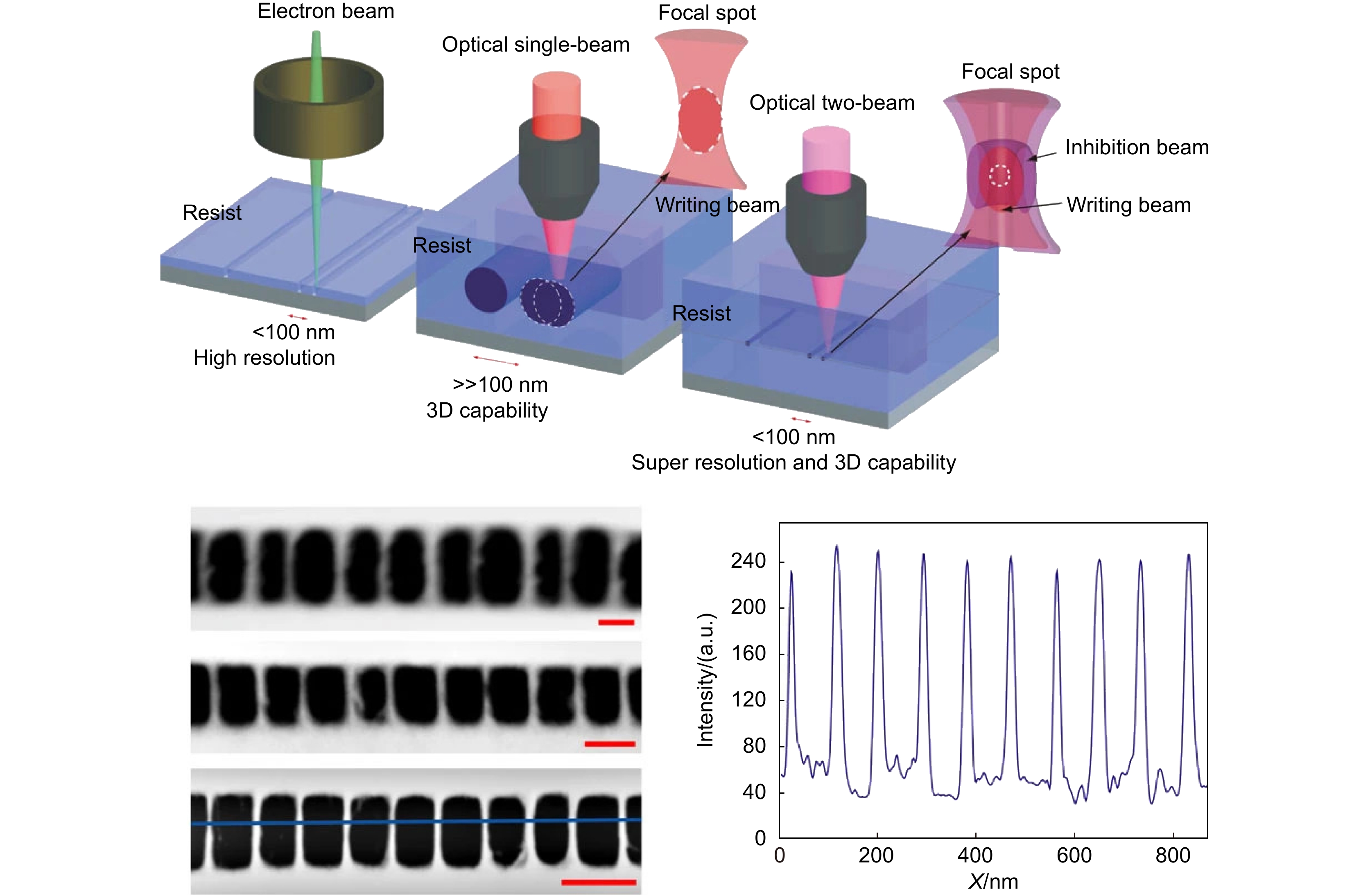
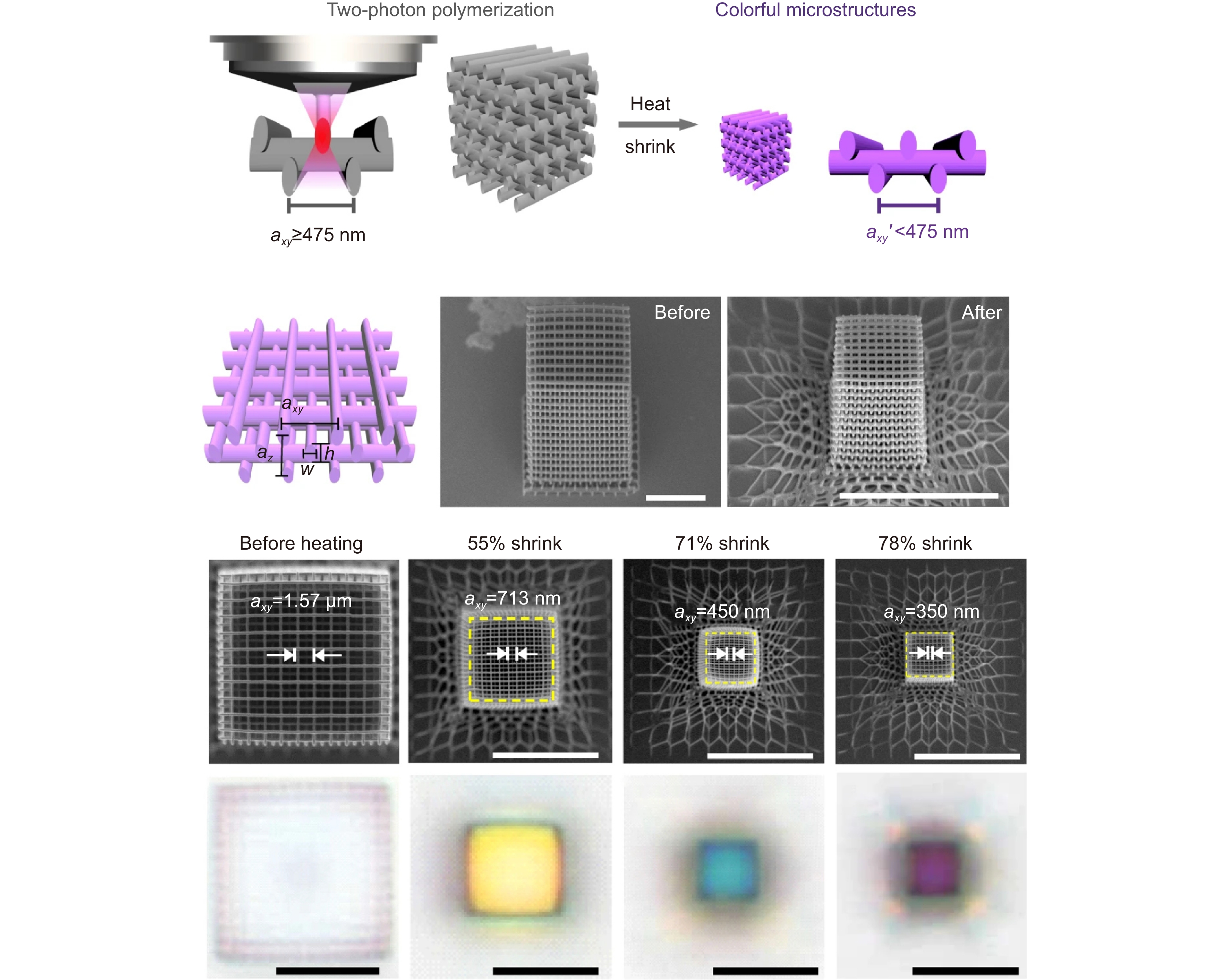
Figure 1.
Schematic diagram of the super-resolution processing principle and characteristics after processing[4]. Figure reproduced with permission from ref. [4] © Springer Nature
-
Figure 2.
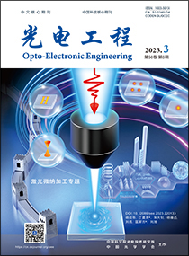
Femtosecond laser direct writing[45]. Figure reproduced with permission from ref. [45] © De Gruyter
-
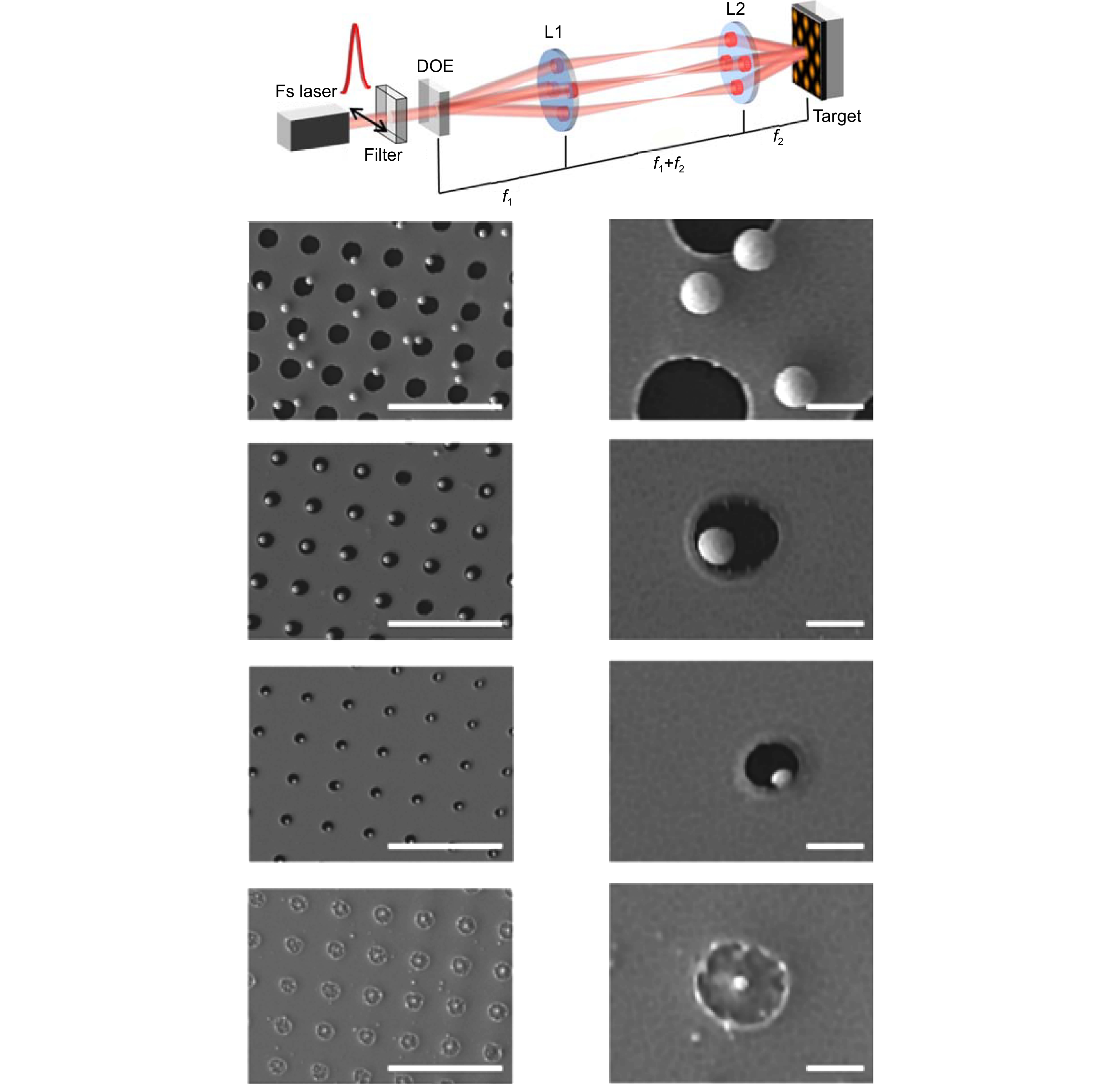
Figure 3.
Schematic diagram of the femtosecond laser fabrication based on diffractive optical elements and characteristics after processing[49]. Figure reproduced with permission from ref. [49] © Springer Nature
-
Figure 4.
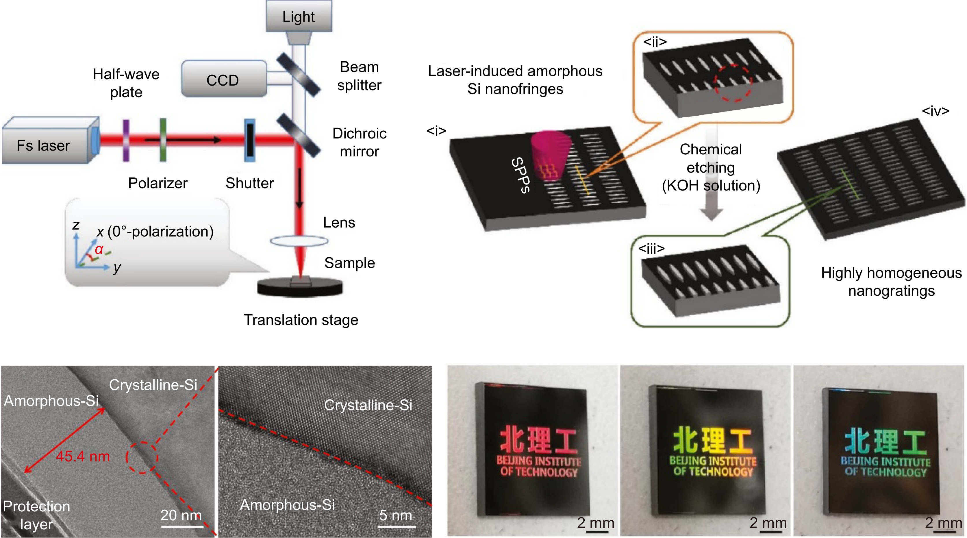
The schematic diagram of the digital micromirror projection system based on femtosecond laser two-photon polymerization and spatio-temporal focusing and characteristics after processing[57]. Figure reproduced with permission from ref. [57] © The American Association for the Advancement of Science(AAAS)
-
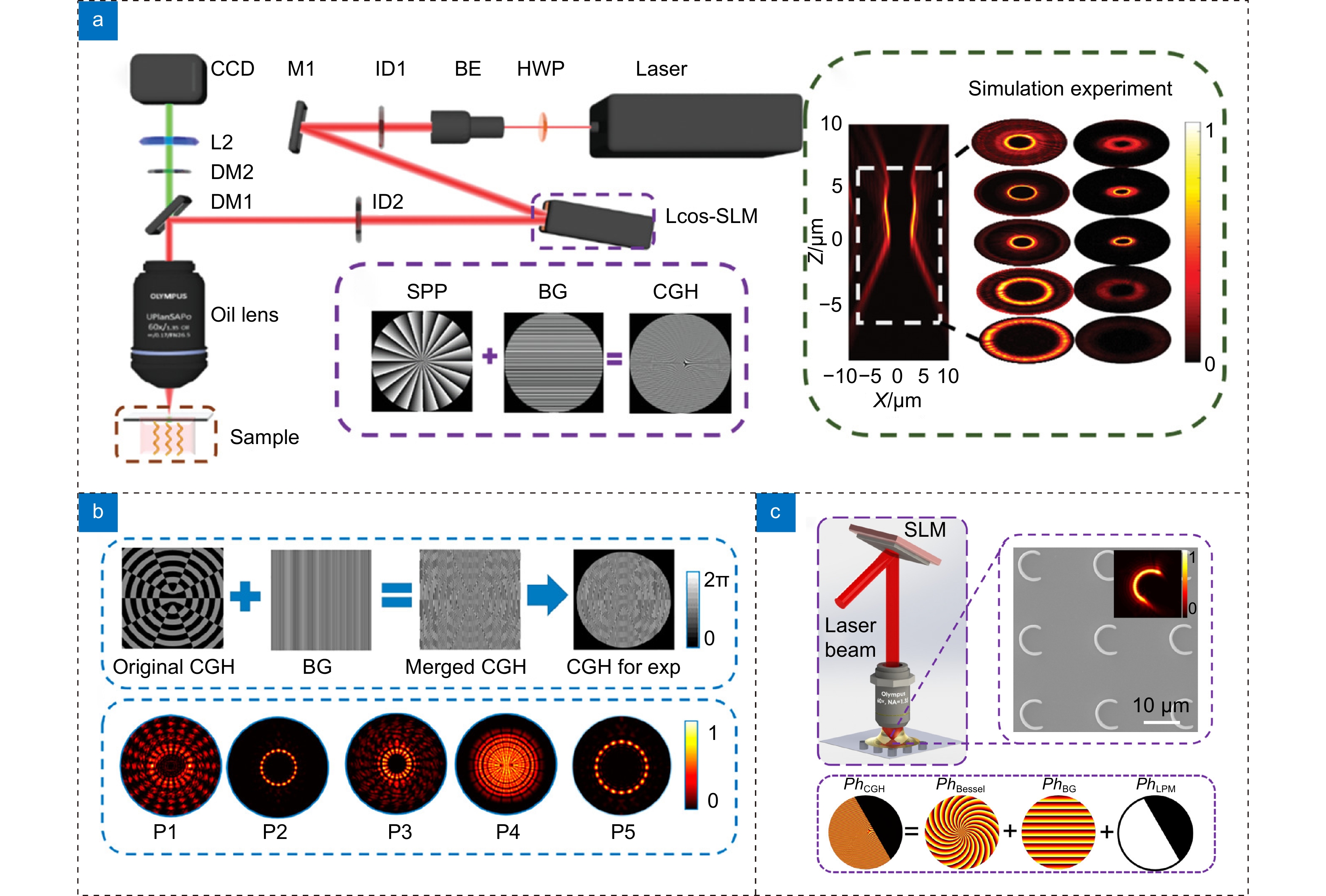
Figure 5.
Parallel processing based on spatial light modulator. (a) Helical scanning of femtosecond ring-shaped vortex beam based on spatial light modulator[65]; (b) Generation of Mathieu beam based on spatial light modulator[66]; (c) Fabrication of microtubes using C-shaped Bessel beam generated by spatial light modulator[68]. Figure reproduced with permission from: (a) ref. [65] © Wiley; (b) ref. [66] and (c) ref. [68] © American Chemical Society.
-
Figure 6.
Focal field engineering based on spatial light modulator[72]. Figure reproduced with permission from ref. [72] © John Wiley and Sons
-
Figure 7.
Schematic diagram of the femtosecond (fs) laser interference processing and characteristics after processing[79]. Figure reproduced with permission from ref. [79] © MDPI
-
Figure 8.
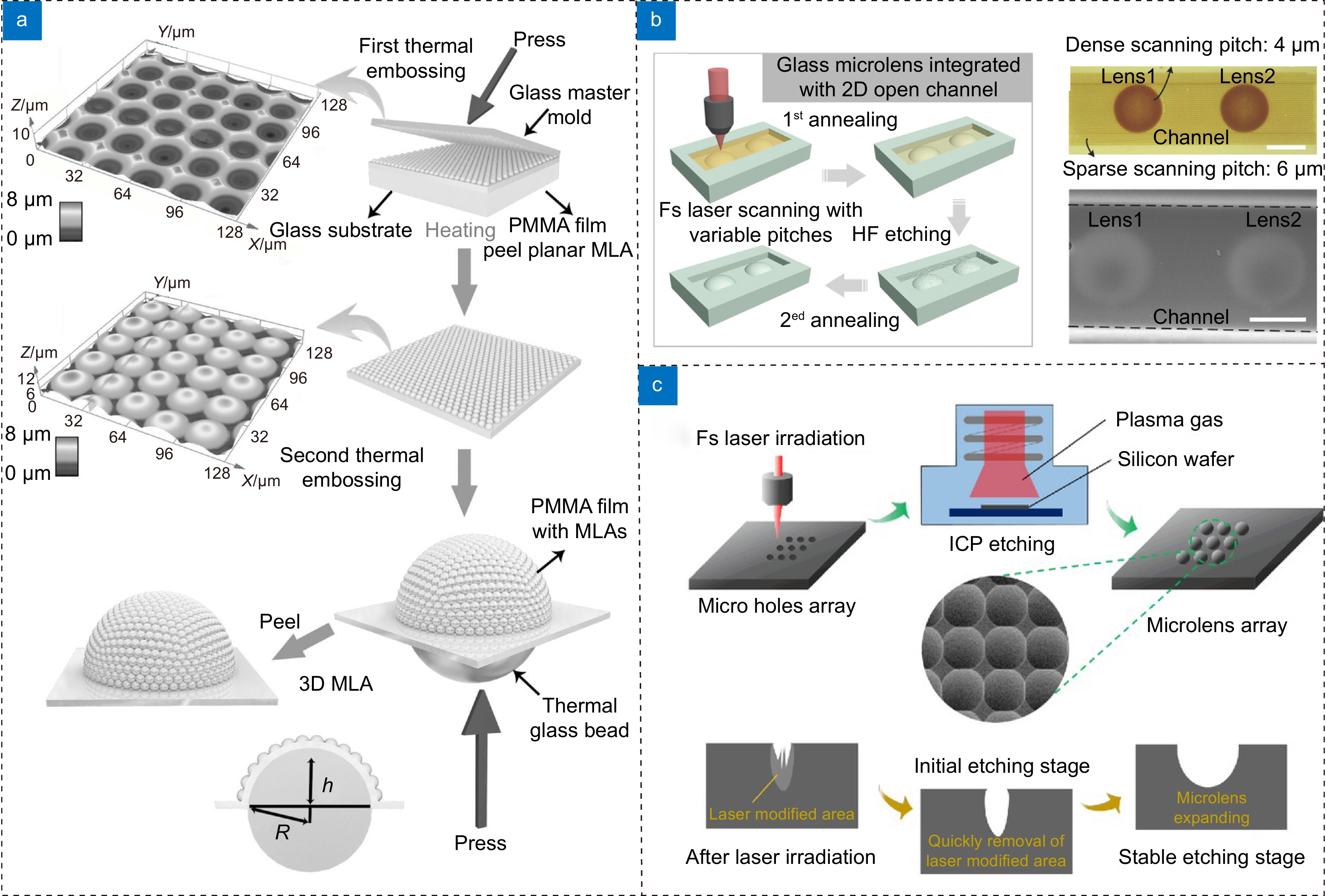
Processing of microlenses. (a) Transferring[83]; (b) Wet etching[84]; (c) Dry etching[86]. Figure reproduced with permission from: (a) ref. [83], (b) ref. [84] and (c) ref. [86] © Wiley
-
Figure 9.
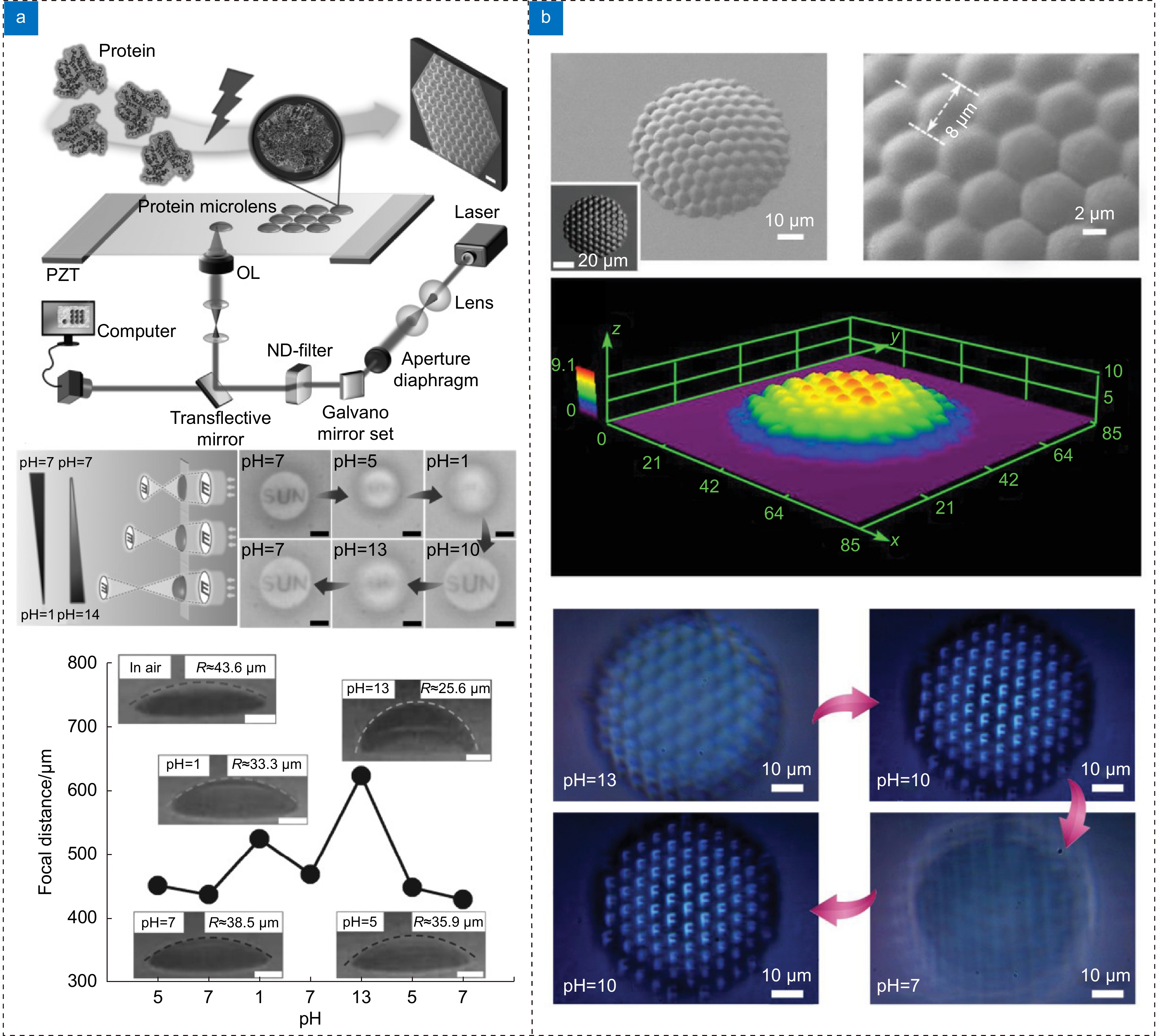
Micromachining of microlenses based on two-photon polymerization of femtosecond laser. (a) Protein-based microlens in response to the change of pH[93]; (b) Double-material compound eye in response to the change of pH[25]. Figure reproduced with permission from: (a) ref. [93] and (b) ref. [25] © Wiley
-
Figure 10.
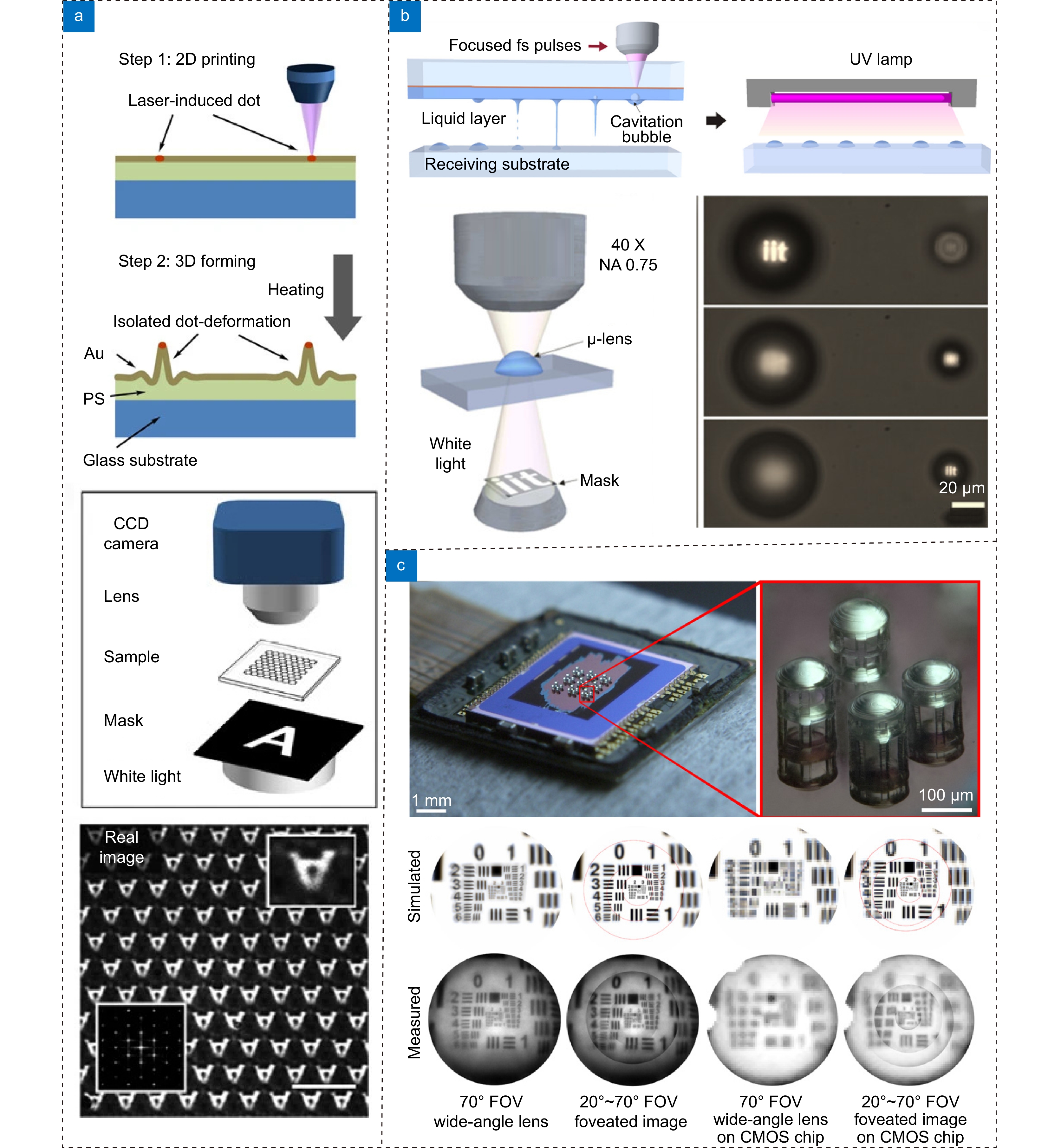
Innovative microlenses. (a) Complex microlens arrays based on laser-induced thermal deformation[95]; (b) Direct patterning of polymeric microlenses based on the combination of femtosecond laser and surface tension of droplet[96]; (c) Integration of compound lens on the surface of CMOS image sensor based on femtosecond laser[82]. Figure reproduced with permission from: (a) ref.[95] © Springer Nature; (b) ref. [96] © American Chemical Society; (c) ref. [82] © The American Association for the Advancement of Science (AAAS)
-
Figure 11.
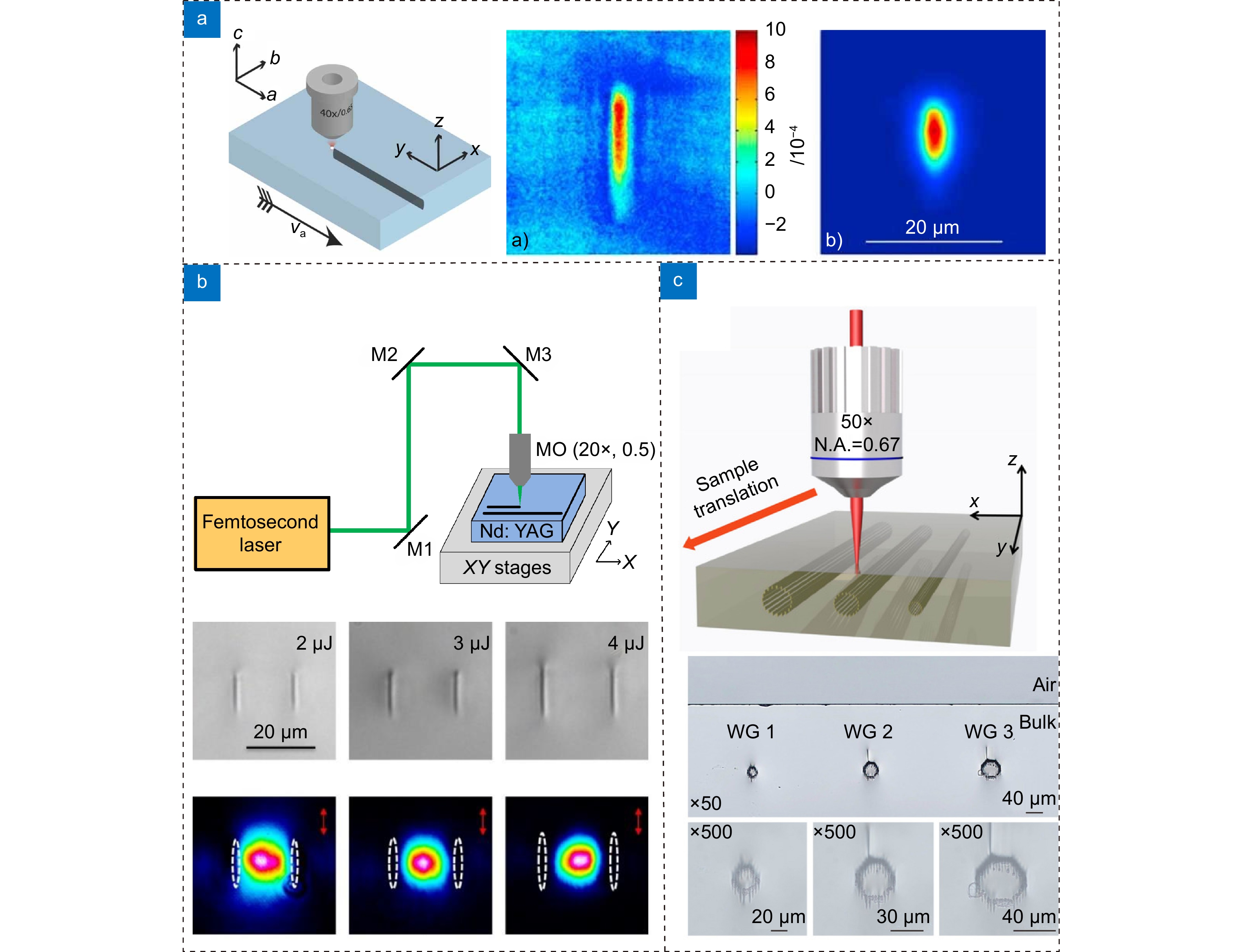
Femtosecond laser direct writing optical waveguide. (a) Single-line waveguide[100]; (b) Double-line waveguide[106]; (c) Depressed cladding waveguide[111]. Figure reproduced with permission from: (a) ref. [100] and (c) ref. [111] © Wiley; (b) ref. [106] © MDPI.
-
Figure 12.
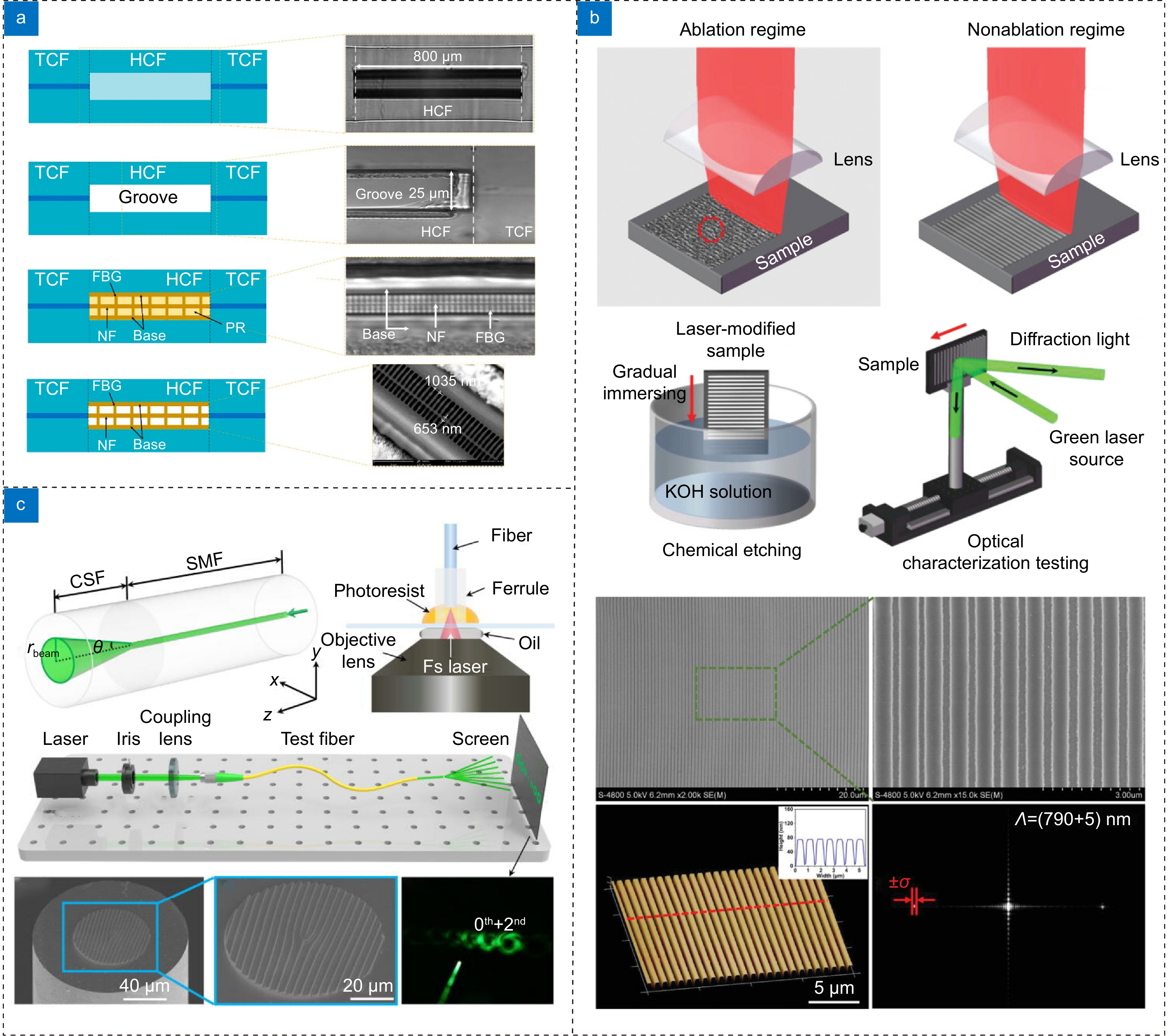
Fabrication of micro-gratings based on femtosecond laser. (a) Procedures of femtosecond laser fabricating FBG[117]; (b) Fabrication of LIPSS on Si substrate utilizing cylindrical lens based on femt osecond laser[129]; (c) Fabrication of continuous phase vortex grating based on two-photon polymerization of femtosecond laser[22]. Figure reproduced with permission from: (a) ref. [117] © American Chemical Society; (b) ref. [129] © Wiley; (c) ref. [22] © AIP Publishing
-
Figure 13.
Fabrication of woodpile photonic crystal whose stop band lies in the visible spectrum based on femtosecond laser[146]. Figure reproduced with permission from ref. [146] © Springer Nature
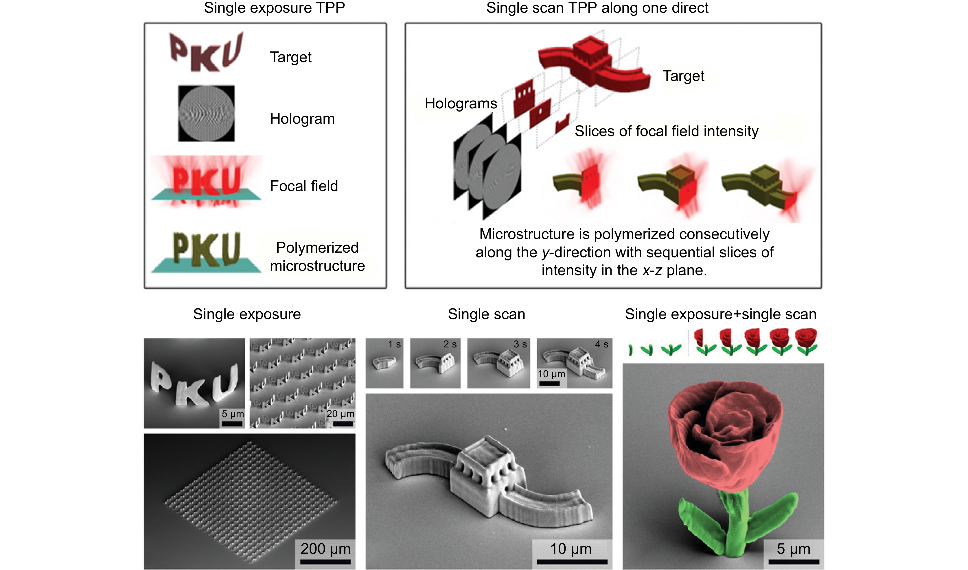
-
Figure 14.
Fabrication of nonlinear photonic crystal based on femtosecond laser. (a) Fabrication of nonlinear photonic crystal in LiNbO3[150]; (b) Fabrication of nonlinear photonic crystal in BCT[151]. Figure reproduced with permission from: (a) ref. [150] and (b) ref. [151] © Springer Nature
- Figure .


