
 E-mail Alert
 RSS
RSS
| Citation: |
Yang S H, Ding C L, Zhu D Z, et al. High-speed two-photon lithography based on femtosecond laser[J]. Opto-Electron Eng, 2023, 50(3): 220133. doi: 10.12086/oee.2023.220133

|
High-speed two-photon lithography based on femtosecond laser
-
Abstract
Two-photon polymerization (TPP) based on femtosecond laser has been a research hotspot in 3D micro/nano writing technology. With the increasing demand for processing complex and large-scale miniaturized 3D devices in the fields of life science, material engineering, micro and nano optics, and etc., the issue of low processing efficiency of TPP is becoming increasingly serious. During the long fabrication period, many disturbances can be introduced in the processing, causing the quality deterioration of the structure and seriously hindering the further popularization and application of these crucial 3D devices. This paper respectively compares the four approaches of single-beam writing, parallel multi-beam writing, pattern projection, and 3D projection exposure based on the TPP lithography efficiency. Moreover, the researches on the optical design of system, the writing accuracy, the fabrication throughput, the writing strategy, and etc. of each approach are also described. And the advantages and disadvantages of these four methods are summerized simultaneously. Finally, we also made a brief prospect to the developing trend of TPL efficiency improvement in the future. -

-
References
[1] Fang L M, Qiao Z, Zhang J, et al. Study on micromachining of femtosecond laser biomedical polymer materials[J]. Key Eng Mater, 2020, 852: 109−118. doi: 10.4028/www.scientific.net/KEM.852.109 [2] Huang R T, Knox W H. Quantitative photochemical scaling model for femtosecond laser micromachining of ophthalmic hydrogel polymers: effect of repetition rate and laser power in the four photon absorption limit[J]. Opt Mater Express, 2019, 9(3): 1049−1061. doi: 10.1364/OME.9.001049 [3] Balbus G H, Echlin M P, Grigorian C M, et al. Femtosecond laser rejuvenation of nanocrystalline metals[J]. Acta Mater, 2018, 156: 183−195. doi: 10.1016/j.actamat.2018.06.027 [4] Kudryashov S I, Levchenko A O, Danilov P A, et al. Direct femtosecond-laser writing of optical-range nanoscale metagratings/metacouplers on diamond surfaces[J]. Appl Phys Lett, 2019, 115(7): 073102. doi: 10.1063/1.5114630 [5] Li W J, Zheng J Q, Zhang Y P, et al. Temperature and depth evaluation of the in vitro effects of femtosecond laser on oral soft tissue, with or without air-cooling[J]. Lasers Med Sci, 2019, 34(4): 649−658. doi: 10.1007/s10103-018-2634-2 [6] Wang L, Chen Q D, Cao X W, et al. Plasmonic nano-printing: large-area nanoscale energy deposition for efficient surface texturing[J]. Light Sci Appl, 2017, 6(12): e17112. doi: 10.1038/lsa.2017.112 [7] Sugioka K, Cheng Y. Femtosecond laser three-dimensional micro-and nanofabrication[J]. J Appl Phys, 2014, 1(4): 041303. doi: 10.1063/1.4904320 [8] Baldacchini T. Three-Dimensional Microfabrication Using Two-Photon Polymerization[M]. 2nd ed. Norwich: William Andrew, 2020. [9] Ahmmed K M T, Grambow C, Kietzig A M. Fabrication of micro/nano structures on metals by femtosecond laser micromachining[J]. Micromachines, 2014, 5(4): 1219−1253. doi: 10.3390/mi5041219 [10] Maruo S, Nakamura O, Kawata K. Three-dimensional microfabrication with two-photon-absorbed photopolymerization[J]. Opt Lett, 1997, 22(2): 132−134. doi: 10.1364/ol.22.000132 [11] Blaicher M, Billah M R, Kemal J, et al. Hybrid multi-chip assembly of optical communication engines by in situ 3D nano-lithography[J]. Light Sci Appl, 2020, 9(1): 71. doi: 10.1038/s41377-020-0272-5 [12] Rhee H W, Shim J, Kim J Y, et al. Direct optical wire bonding through open-to-air polymerization for silicon photonic chips[J]. Opt Lett, 2022, 47(3): 714−717. doi: 10.1364/OL.445526 [13] Khorasaninejad M, Chen W T, Devlin R C, et al. Metalenses at visible wavelengths: diffraction-limited focusing and subwavelength resolution imaging[J]. Science, 2016, 352(6290): 1190−1194. doi: 10.1126/science.aaf6644 [14] Agrawal L, Saidani M, Guillaud L, et al. Development of 3D culture scaffolds for directional neuronal growth using 2-photon lithography[J]. Mater Sci Eng C, 2021, 131: 112502. doi: 10.1016/j.msec.2021.112502 [15] Jayne R K, Karakan M Ç, Zhang K H, et al. Direct laser writing for cardiac tissue engineering: a microfluidic heart on a chip with integrated transducers[J]. Lab Chip, 2021, 21(9): 1724−1737. doi: 10.1039/D0LC01078B [16] Sanli U T, Messer T, Weigand M, et al. High-resolution kinoform X-ray optics printed via 405 nm 3D laser lithography[J]. Adv Mater Technol, 2022,doi: 10.1002/admt.202101695. [17] Fischer J, von Freymann G, Wegener M. The materials challenge in diffraction-unlimited direct-laser-writing optical lithography[J]. Adv Mater, 2010, 22(32): 3578−3582. doi: 10.1002/adma.201000892 [18] Fischer J, Wegener M. Three-dimensional direct laser writing inspired by stimulated-emission-depletion microscopy [Invited][J]. Opt Mater Express, 2011, 1(4): 614−624. doi: 10.1364/OME.1.000614 [19] Müller P, Müller R, Hammer L, et al. STED-inspired laser lithography based on photoswitchable spirothiopyran moieties[J]. Chem Mater, 2019, 31(6): 1966−1972. doi: 10.1021/acs.chemmater.8b04696 [20] Sankaranarayanan J, Muthukrishnan S, Gudmundsdottir A D. Photoremovable protecting groups based on photoenolization[J]. Adv Phys Org Chem, 2009, 43: 39−77. doi: 10.1016/S0065-3160(08)00002-6 [21] Cao C, Liu J T, Xia X M, et al. Click chemistry assisted organic-inorganic hybrid photoresist for ultra-fast two-photon lithography[J]. Addit Manuf, 2022, 51: 102658. doi: 10.1016/j.addma.2022.102658 [22] 曹春, 邱毅伟, 刘建亭, 等. 聚乙烯吡咯烷酮杂化双色光敏激光直写光刻胶研究[J]. 高分子学报, 2022, 53(6): 608−616. doi: 10.11777/j.issn1000-3304.2021.21323 Cao C, Qiu Y W, Liu J T, et al. Polyvinylpyrrolidone hybrid photoresist for two-color sensitive direct laser writing[J]. Acta Polym Sin, 2022, 53(6): 608−616. doi: 10.11777/j.issn1000-3304.2021.21323 [23] Mueller P, Zieger M M, Richter B, et al. Molecular switch for sub-diffraction laser lithography by photoenol intermediate-state Cis-trans isomerization[J]. ACS Nano, 2017, 11(6): 6396−6403. doi: 10.1021/acsnano.7b02820 [24] Netto-Ferreira J C, Scaiano J C. A laser flash photolysis study of the mechanism of the photocyclization of ɑ-chloro-o-methylacetophenones[J]. J Am Chem Soc, 1991, 113(15): 5800−5803. doi: 10.1021/ja00015a038 [25] Gruendling T, Oehlenschlaeger K K, Frick E, et al. Rapid UV light-triggered macromolecular click conjugations via the use of o-quinodimethanes[J]. Macromol Rapid Commun, 2011, 32(11): 807−812. doi: 10.1002/marc.201100159 [26] Kathan M, Hecht S. Photoswitchable molecules as key ingredients to drive systems away from the global thermodynamic minimum[J]. Chem Soc Rev, 2017, 46(18): 5536−5550. doi: 10.1039/C7CS00112F [27] Bertrand O, Gohy J F. Photo-responsive polymers: synthesis and applications[J]. Polym Chem, 2017, 8(1): 52−73. doi: 10.1039/C6PY01082B [28] Ding C L, Zhu D Z, Wei Z, et al. A compact and high-precision method for active beam stabilization system[J]. Opt Commun, 2021, 500: 127328. doi: 10.1016/j.optcom.2021.127328 [29] Hell S W, Wichmann J. Breaking the diffraction resolution limit by stimulated emission: stimulated-emission-depletion fluorescence microscopy[J]. Opt Lett, 1994, 19(11): 780−782. doi: 10.1364/OL.19.000780 [30] Saha S K, Wang D E, Nguyen V H, et al. Scalable submicrometer additive manufacturing[J]. Science, 2019, 366(6461): 105−109. doi: 10.1126/science.aax8760 [31] Pawlicki M, Collins H A, Denning R G, et al. Two-photon absorption and the design of two-photon dyes[J]. Angew Chem Int Ed, 2009, 48(18): 3244−3266. doi: 10.1002/anie.200805257 [32] Gu J, Yulan W, Chen W Q, et al. Carbazole-based 1D and 2D hemicyanines: synthesis, two-photon absorption properties and application for two-photon photopolymerization 3D lithography[J]. New J Chem, 2007, 31(1): 63−68. doi: 10.1039/B609309D [33] Xing J F, Chen W Q, Gu J, et al. Design of high efficiency for two-photon polymerization initiator: combination of radical stabilization and large two-photon cross-section achieved by N-benzyl 3, 6-bis (phenylethynyl) carbazole derivatives[J]. J Mater Chem, 2007, 17(14): 1433−1438. doi: 10.1039/b616792f [34] Cao X B, Jin F, Li Y F, et al. Triphenylamine-modified quinoxaline derivatives as two-photon photoinitiators[J]. New J Chem, 2009, 33(7): 1578−1582. doi: 10.1039/b900464e [35] Holzer B, Lunzer M, Rosspeintner A, et al. Towards efficient initiators for two-photon induced polymerization: fine tuning of the donor/acceptor properties[J]. Mol Syst Des Eng, 2019, 4(2): 437−448. doi: 10.1039/c8me00101d [36] Chi T, Somers P, Wilcox D A, et al. Tailored thioxanthone-based photoinitiators for two-photon-controllable polymerization and nanolithographic printing[J]. J Polym Sci Part B Polym Phys, 2019, 57(21): 1462−1475. doi: 10.1002/polb.24891 [37] Hu P, Qiu W W, Naumov S, et al. Conjugated bifunctional carbazole-based oxime esters: efficient and versatile photoinitiators for 3D printing under one-and two-photon excitation[J]. Chem Photo Chem, 2020, 4(3): 224−232. doi: 10.1002/cptc.201900246 [38] Li Z Q, Pucher N, Cicha K, et al. A straightforward synthesis and structure-activity relationship of highly efficient initiators for two-photon polymerization[J]. Macromolecules, 2013, 46(2): 352−361. doi: 10.1021/ma301770a [39] He M F, Zhang Z M, Cao C, et al. 3D sub-diffraction printing by multicolor photoinhibition lithography: from optics to chemistry[J]. Laser Photonics Rev, 2022, 16(2): 2100229. doi: 10.1002/LPOR.202100229 [40] Chen S, Zheng M L, Dong X Z, et al. Nondegenerate two-photon absorption in a zinc blende-type ZnS single crystal using the femtosecond pump-probe technique[J]. J Opt Soc Am B, 2013, 30(12): 3117−3122. doi: 10.1364/JOSAB.30.003117 [41] Chen S, Zheng Y C, Zheng M L, et al. Nondegenerate two-photon absorption properties of a newly synthesized carbazole derivative[J]. J Mater Chem C, 2017, 5(2): 470−475. doi: 10.1039/C6TC04676B [42] Yoo H W, Ito S, Schitter G. High speed laser scanning microscopy by iterative learning control of a galvanometer scanner[J]. Control Eng Pract, 2016, 50: 12−21. doi: 10.1016/j.conengprac.2016.02.007 [43] 唐建波. 基于光束扫描的共焦显微三维测量技术研究[D]. 哈尔滨: 哈尔滨工业大学, 2011. Tang J B. Three dimensional confocal imaging based on beam scanning technology[D]. Harbin: Harbin Institute of Technology, 2011. [44] De Loor R. Polygon scanner system for ultra short pulsed laser micro-machining applications[J]. Phys Procedia, 2013, 41: 544−551. doi: 10.1016/j.phpro.2013.03.114 [45] Schille J, Schneider L, Streek A, et al. High-throughput machining using a high-average power ultrashort pulse laser and high-speed polygon scanner[J]. Opt Eng, 2016, 55(9): 096109. doi: 10.1117/1.OE.55.9.096109 [46] Iyer V, Hoogland T M, Saggau P. Fast functional imaging of single neurons using random-access multiphoton (RAMP) microscopy[J]. J Neurophysiol, 2006, 95(1): 535−545. doi: 10.1152/jn.00865.2005 [47] Grewe B F, Langer D, Kasper H, et al. High-speed in vivo calcium imaging reveals neuronal network activity with near-millisecond precision[J]. Nat Methods, 2010, 7(5): 399−405. doi: 10.1038/nmeth.1453 [48] Lechleiter J D, Lin D T, Sieneart I. Multi-photon laser scanning microscopy using an acoustic optical deflector[J]. Biophys J, 2002, 83(4): 2292−2299. doi: 10.1016/S0006-3495(02)73989-1 [49] Roorda R D, Hohl T M, Toledo-Crow R, et al. Video-rate nonlinear microscopy of neuronal membrane dynamics with genetically encoded probes[J]. J Neurophysiol, 2004, 92(1): 609−621. doi: 10.1152/jn.00087.2004 [50] Iyer V, Losavio B E, Saggau P. Compensation of spatial and temporal dispersion for acousto-optic multiphoton laser-scanning microscopy[J]. J Biomed Opt, 2003, 8(3): 460−471. doi: 10.1117/1.1580827 [51] Salomé R, Kremer Y, Dieudonné S, et al. Ultrafast random-access scanning in two-photon microscopy using acousto-optic deflectors[J]. J Neurosci Methods, 2006, 154(1–2): 161−174. doi: 10.1016/j.jneumeth.2005.12.010 [52] Kirkpatrick S M, Baur J W, Clark C M, et al. Holographic recording using two-photon-induced photopolymerization[J]. Appl Phys A, 1999, 69(4): 461−464. doi: 10.1007/s003390051033 [53] Matsuo S, Kondo T, Juodkazis S, et al. Fabrication of three-dimensional photonic crystals by femtosecond laser interference[J]. Proc SPIE, 2002, 4655: 327−334. doi: 10.1117/12.463891 [54] Kondo T, Matsuo S, Juodkazis S, et al. Multiphoton fabrication of periodic structures by multibeam interference of femtosecond pulses[J]. Appl Phys Lett, 2003, 82(17): 2758−2760. doi: 10.1063/1.1569987 [55] Kondo T, Juodkazis S, Mizeikis V, et al. Fabrication of three-dimensional periodic microstructures in photoresist SU-8 by phase-controlled holographic lithography[J]. New J Phys, 2006, 8(10): 250. doi: 10.1088/1367-2630/8/10/250 [56] Stankevičius E, Malinauskas M, Gedvilas M, et al. Fabrication of periodic micro-structures by multi-photon polymerization using the femtosecond laser and four-beam interference[J]. Mater Sci, 2011, 17(3): 244−248. doi: 10.5755/j01.ms.17.3.587 [57] Girsault A, Meller A. Sub-second, super-resolved imaging of biological systems using parallel EO-STED[J]. Opt Lett, 2020, 45(10): 2712−2715. doi: 10.1364/OL.392822 [58] Bergermann F, Alber L, Sahl S J, et al. 2000-fold parallelized dual-color STED fluorescence nanoscopy[J]. Opt Express, 2015, 23(1): 211−223. doi: 10.1364/OE.23.000211 [59] Yang B, Fang C Y, Chang H C, et al. Polarization effects in lattice-STED microscopy[J]. Faraday Discuss, 2015, 184: 37−49. doi: 10.1039/c5fd00092k [60] Li D, Shao L, Chen B C, et al. Extended-resolution structured illumination imaging of endocytic and cytoskeletal dynamics[J]. Science, 2015, 349(6251): 527. doi: 10.1126/science.aab3500 [61] Förster R, Lu-Walther H W, Jost A, et al. Simple structured illumination microscope setup with high acquisition speed by using a spatial light modulator[J]. Opt Express, 2014, 22(17): 20663−20677. doi: 10.1364/OE.22.020663 [62] Chmyrov A, Keller J, Grotjohann T, et al. Nanoscopy with more than 100, 000 'doughnuts'[J]. Nat Methods, 2013, 10(8): 737−740. doi: 10.1038/nmeth.2556 [63] Tang M, Chen Z C, Huang Z Q, et al. Maskless multiple-beam laser lithography for large-area nanostructure/microstructure fabrication[J]. Appl Opt, 2011, 50(35): 6536−6542. doi: 10.1364/AO.50.006536 [64] Matsuo S, Juodkazis S, Misawa H. Femtosecond laser microfabrication of periodic structures using a microlens array[J]. Appl Phys A, 2005, 80(4): 683−685. doi: 10.1007/s00339-004-3108-x [65] Kato J I, Takeyasu N, Adachi Y, et al. Multiple-spot parallel processing for laser micronanofabrication[J]. Appl Phys Lett, 2005, 86(4): 044102. doi: 10.1063/1.1855404 [66] Formanek F, Takeyasu N, Tanaka T, et al. Three-dimensional fabrication of metallic nanostructures over large areas by two-photon polymerization[J]. Opt Express, 2006, 14(2): 800−809. doi: 10.1364/OPEX.14.000800 [67] Račiukaitis G, Stankevičius E, Gečys P, et al. Laser processing by using diffractive optical laser beam shaping technique[J]. JLMN-J Laser Micro/Nanoeng, 2011, 6(1): 37−43. doi: 10.2961/jlmn.2011.01.0009 [68] Hilton P A, Lloyd D, Tyrer J R. Use of a diffractive optic for high power laser cutting[J]. J Laser Appl, 2016, 28(1): 012014. doi: 10.2351/1.4938279 [69] Kuchmizhak A A, Porfirev A P, Syubaev S A, et al. Multi-beam pulsed-laser patterning of plasmonic films using broadband diffractive optical elements[J]. Opt Lett, 2017, 42(14): 2838−2841. doi: 10.1364/OL.42.002838 [70] Kwon H H, Yang S H, Cho Y J, et al. Comparison of a 1064-nm neodymium‐doped yttrium aluminum garnet picosecond laser using a diffractive optical element vs. a nonablative 1550-nm erbium-glass laser for the treatment of facial acne scarring in Asian patients: a 17-week prospective, randomized, split-face, controlled trial[J]. J Eur Acad Dermatol Venereol, 2020, 34(12): 2907−2913. doi: 10.1111/jdv.16643 [71] Vandenhouten R, Hermerschmidt A, Fiebelkorn R. Design and quality metrics of point patterns for coded structured light illumination with diffractive optical elements in optical 3D sensors[J]. Proc SPIE, 2017, 10335: 1033518. doi: 10.1117/12.2270248 [72] Dong X Z, Zhao Z S, Duan X M. Micronanofabrication of assembled three-dimensional microstructures by designable multiple beams multiphoton processing[J]. Appl Phys Lett, 2007, 91(12): 124103. doi: 10.1063/1.2789661 [73] Hahn V, Kiefer P, Frenzel T, et al. Rapid assembly of small materials building blocks (voxels) into large functional 3D metamaterials[J]. Adv Funct Mater, 2020, 30(26): 1907795. doi: 10.1002/adfm.201907795 [74] Gittard S D, Nguyen A, Obata K, et al. Fabrication of microscale medical devices by two-photon polymerization with multiple foci via a spatial light modulator[J]. Biomed Opt Express, 2011, 2(11): 3167−3178. doi: 10.1364/BOE.2.003167 [75] Yang L, El-Tamer A, Hinze U, et al. Parallel direct laser writing of micro-optical and photonic structures using spatial light modulator[J]. Opt Lasers Eng, 2015, 70: 26−32. doi: 10.1016/j.optlaseng.2015.02.006 [76] Li X P, Cao Y Y, Tian N, et al. Multifocal optical nanoscopy for big data recording at 30 TB capacity and gigabits/second data rate[J]. Optica, 2015, 2(6): 567−570. doi: 10.1364/OPTICA.2.000567 [77] Xu B, Du W Q, Li J W, et al. High efficiency integration of three-dimensional functional microdevices inside a microfluidic chip by using femtosecond laser multifoci parallel microfabrication[J]. Sci Rep, 2016, 6(1): 19989. doi: 10.1038/srep19989 [78] Hu Y L, Feng W F, Xue C, et al. Self-assembled micropillars fabricated by holographic femtosecond multi-foci beams for in situ trapping of microparticles[J]. Opt Lett, 2020, 45(17): 4698−4701. doi: 10.1364/OL.398682 [79] Geng Q, Wang D E, Chen P F, et al. Ultrafast multi-focus 3-D nano-fabrication based on two-photon polymerization[J]. Nat Commun, 2019, 10(1): 2179. doi: 10.1038/s41467-019-10249-2 [80] Mills B, Grant-Jacob J A, Feinaeugle M, et al. Single-pulse multiphoton polymerization of complex structures using a digital multimirror device[J]. Opt Express, 2013, 21(12): 14853−14858. doi: 10.1364/OE.21.014853 [81] Aagedal H, Schmid M, Beth T, et al. Theory of speckles in diffractive optics and its application to beam shaping[J]. J Mod Opt, 1996, 43(7): 1409−1421. doi: 10.1080/09500349608232814 [82] Zhang C C, Hu Y L, Li J W, et al. An improved multi-exposure approach for high quality holographic femtosecond laser patterning[J]. Appl Phys Lett, 2014, 105(22): 221104. doi: 10.1063/1.4902925 [83] Aharoni T, Shoham S. Phase-controlled, speckle-free holographic projection with applications in precision optogenetics[J]. Neurophotonics, 2018, 5(2): 025004. doi: 10.1117/1.NPh.5.2.025004 [84] Wang Z P, Li X W, Jiang L, et al. High-quality micropattern printing by interlacing-pattern holographic femtosecond pulses[J]. Nanophotonics, 2020, 9(9): 2895−2904. doi: 10.1515/nanoph-2020-0138 [85] Nomura T, Okamura M, Nitanai E, et al. Image quality improvement of digital holography by superposition of reconstructed images obtained by multiple wavelengths[J]. Appl Opt, 2008, 47(19): D38−D43. doi: 10.1364/AO.47.000D38 [86] Fan H, Cao X W, Wang L, et al. Control of diameter and numerical aperture of microlens by a single ultra-short laser pulse[J]. Opt Lett, 2019, 44(21): 5149−5152. doi: 10.1364/OL.44.005149 [87] Yang L, Hu Z J, Xin C, et al. One-step synthesis of three-dimensional microtubes with single exposure of structured femtosecond optical vortices[J]. Proc SPIE, 2018, 10522: 105221H. doi: 10.1117/12.2289043 [88] Xin C, Yang L, Li J W, et al. Conical hollow microhelices with superior swimming capabilities for targeted cargo delivery[J]. Adv Mater, 2019, 31(25): 1808226. doi: 10.1002/adma.201808226 [89] Yang L, Chen X X, Wang L, et al. Targeted single‐cell therapeutics with magnetic tubular micromotor by one‐step exposure of structured femtosecond optical vortices[J]. Adv Funct Mater, 2019, 29(45): 1905745. doi: 10.1002/adfm.201905745 [90] Pan D, Liu S L, Li J W, et al. Rapid fabrication of 3D chiral microstructures by single exposure of interfered femtosecond vortex beams and capillary-force-assisted self-assembly[J]. Adv Funct Mater, 2022, 32(4): 2106917. doi: 10.1002/adfm.202106917 -
Overview
Two-photon lithography (TPL) has been a research hotspot in 3D micro/nano writing technology due to its characteristics of high resolution, low thermal influence, a wide range of processed materials, low environmental requirements, and 3D processing capability. It has shown unique advantages in the fields of life science, material engineering, micro/nano optics, microfluidic, micro machinery, and so on. This paper summarizes the research works done by researchers on different writing methods to improve TPL processing efficiency. Single-beam writing is the main method for TPL, which mainly depends on the speed of the scanning device. Single-beam writing has the advantages of simple system and high-quality beam, and it is easy to combine various effects to improve writing results. It mainly includes scanning modes based on the translation stage, galvo, polygon laser scanner, and acousto-optic deflector (AOD) (Fig. 2). All these modes have advantages and disadvantages. As for the scanning speed comparison, polygon laser scanner and AOD have relatively faster writing rates (faster than m/s). Multi-foci parallel lithography can obviously promote efficiency, elevating the speed by dozens or even hundreds of thousands of times, mainly based on spatial light modulator (SLM), digital micromirror device (DMD), microlens array (MLA), diffractive optical elements (DOE), multi-beam interference, and so on (Figs. 3-15). Multi-foci parallel lithography based on SLM is most widely used owing to its high efficiency and ability to flexible and independent control of each single beam, but the refresh rate is still insufficient. DMD has a higher refreshing rate (32 kHz), but the state-of-the-art beam parallelism realized by DMD is severely limited. More parallel beams are further required for improving the processing efficiency. The 2D pattern exposure method based on SLM or DMD can further improve the TPL efficiency with the superiority of generating flexibly designed pattern (Figs. 16-18). However, the 2D projection exposure technology is still difficult to achieve high writing precision, especially the axial resolution. An available method to improve the axial precision is spatially and temporally focusing an ultrafast laser to implement a strong intensity gradient at the spatial focal plane that restricts polymerization within a thin layer. The 3D projection method will be the most efficient writing method in the future, especially in 3D device processing (Figs. 19-20). Researchers used this technique to make hollow tubular and conical helices structures, increasing the processing speed by 600 times. However, the research results show that the current 3D projection can only process simple 3D structures. Further researches on 3D exposure processing of complex structures are expected, which will effectively expand its application in various fields. Authors believe that with the effort of researchers on efficiency improvement gradually, TPL can further highlight its advantages to promote the development of life science, materials engineering, micro-nano optics, and many other fields.
-
Access History

Export File
Citation
Yang S H, Ding C L, Zhu D Z, et al. High-speed two-photon lithography based on femtosecond laser[J]. Opto-Electron Eng, 2023, 50(3): 220133. doi: 10.12086/oee.2023.220133
Format
Content
 DownLoad:

-
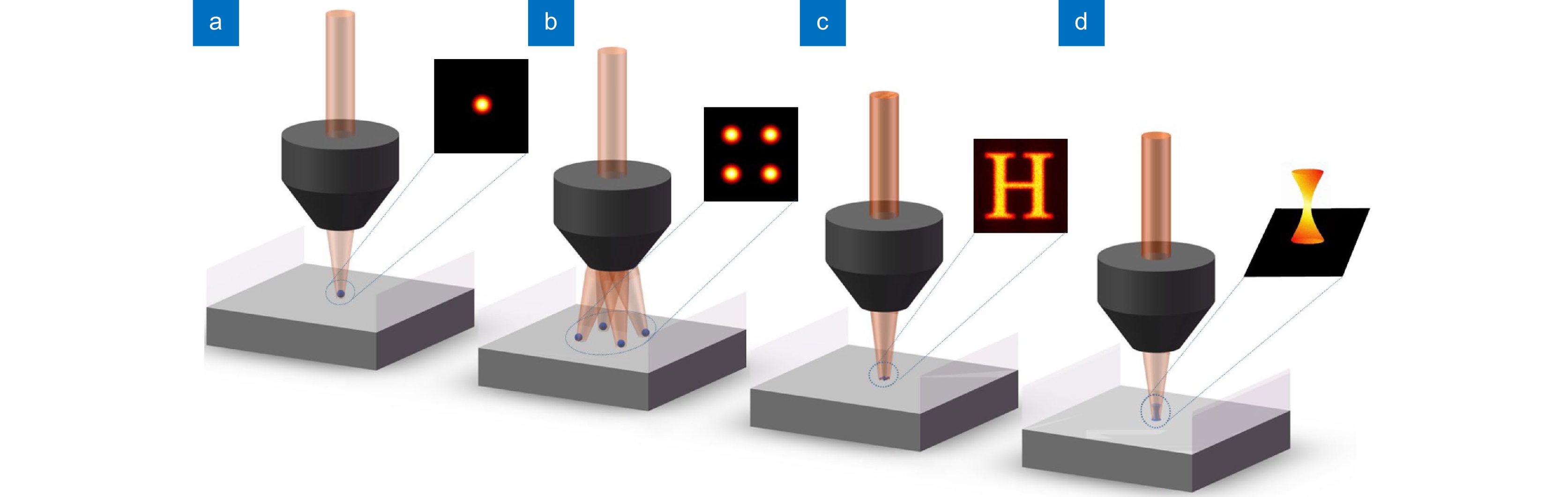
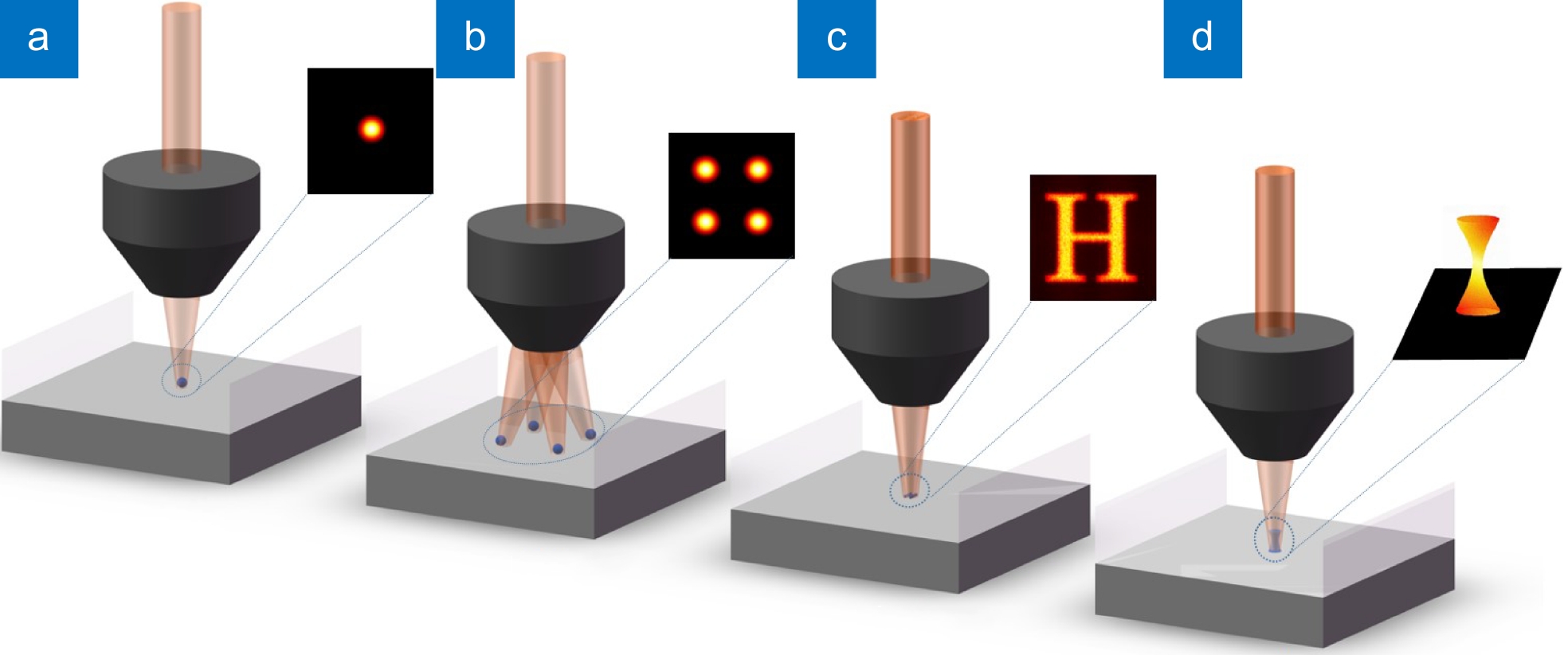
Figure 1.
Optical methods of improving the TPL throughput. (a) Single-beam writing; (b) Multi-foci parallel lithography; (c) Pattern projection; (d) 3D projection exposure
-
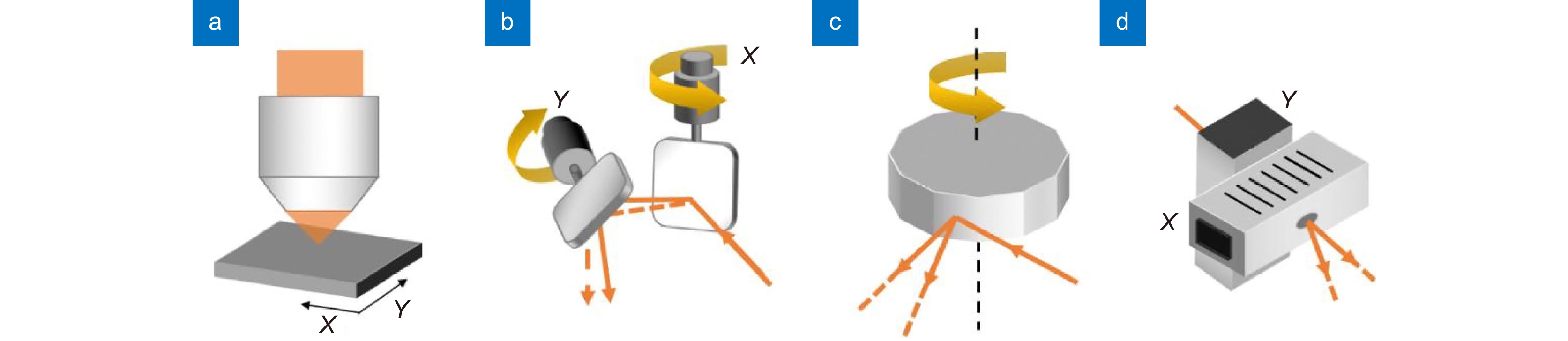
Figure 2.
The scanning scheme for single-beam writing based on (a) motorized stage, (b) galvo, (c) polygon laser scanner, and (d) acousto-optic deflector (AOD)
-
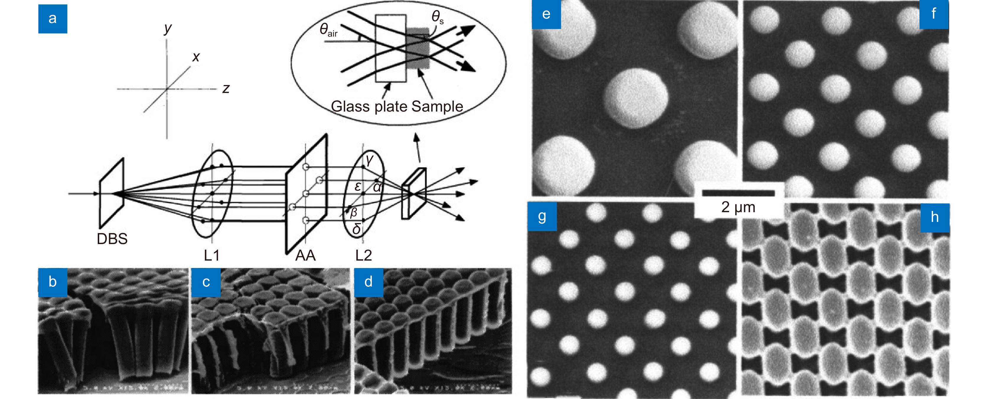
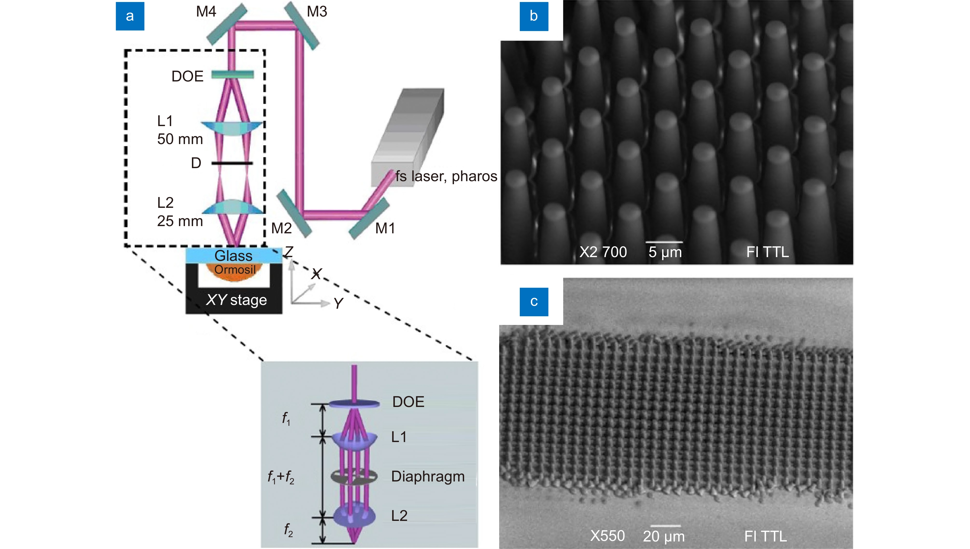
Figure 3.
(a) Configuration of the parallel writing system based on diffractive beam splitter (DBS) and multi-beam interference; (b)~(d) The periodic structures written by the foci array generated via the interference of four femtosecond laser beams (800 nm/1 kHz). The exposure time is 30 s, 80 s, and 120 s, respectively; (e)~(g) The dot array structures fabricated by the foci lattice generated via four-beam interference with different interference angles of 10.8°, 21.9°, and 33.6°, respectively; (h) The periodic lattice structure written by the foci array generated via three-beam interference[53-55]
-
Figure 4.
(a) Configuration of the multi-photon writing system based on four-beam interference; (b) Pillar array fabricated by once laser exposure (1 s), period 7.5 μm, height 20 μm, and diameter 3 μm; (c) Large-scale periodic structure fabricated by continuously shifting the once-exposure position of foci array with diameter of ~80 μm[56]
-
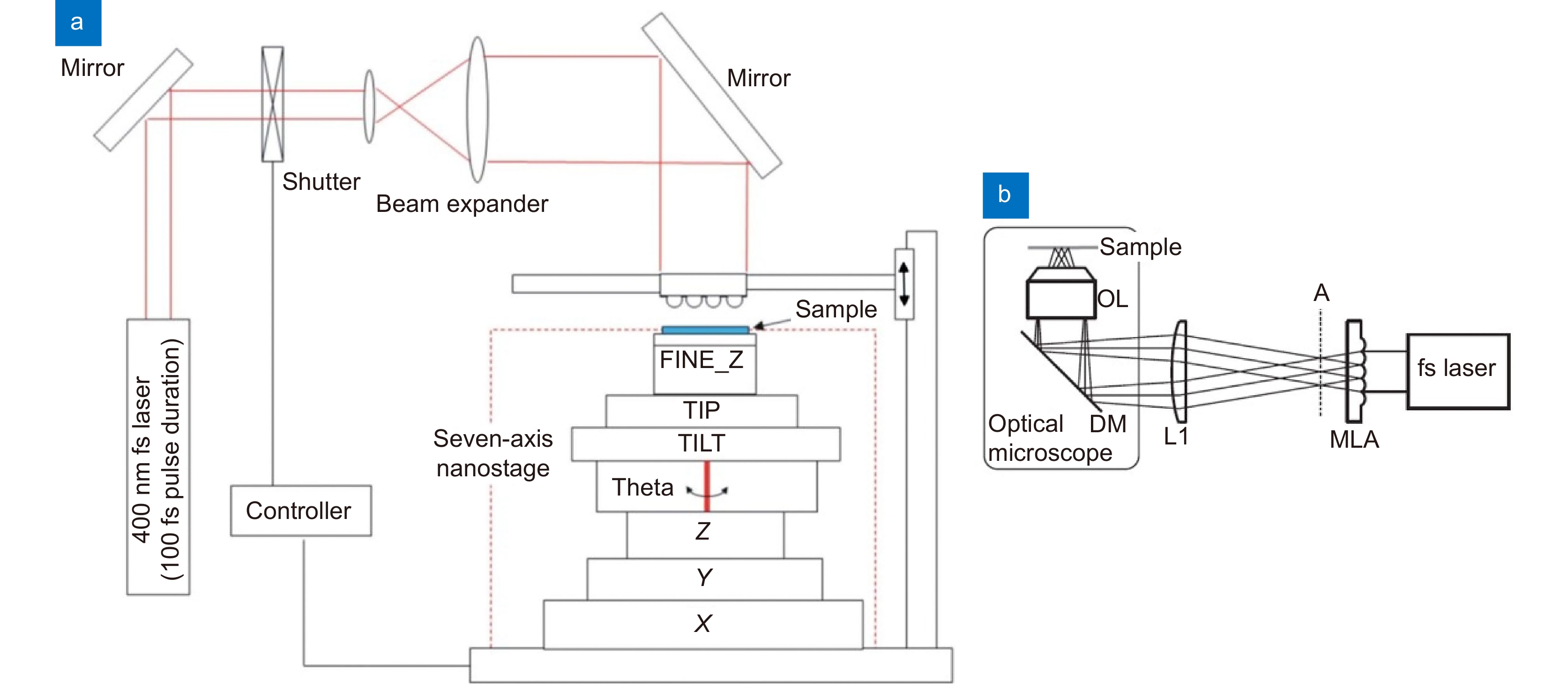
Figure 5.
Femtosecond laser parallel direct writing system based on MLA. (a) Direct writing using MLA foci array; (b) Multi-foci writing by imaging the MLA foci array to the focal plane of the objective[63-64]
-
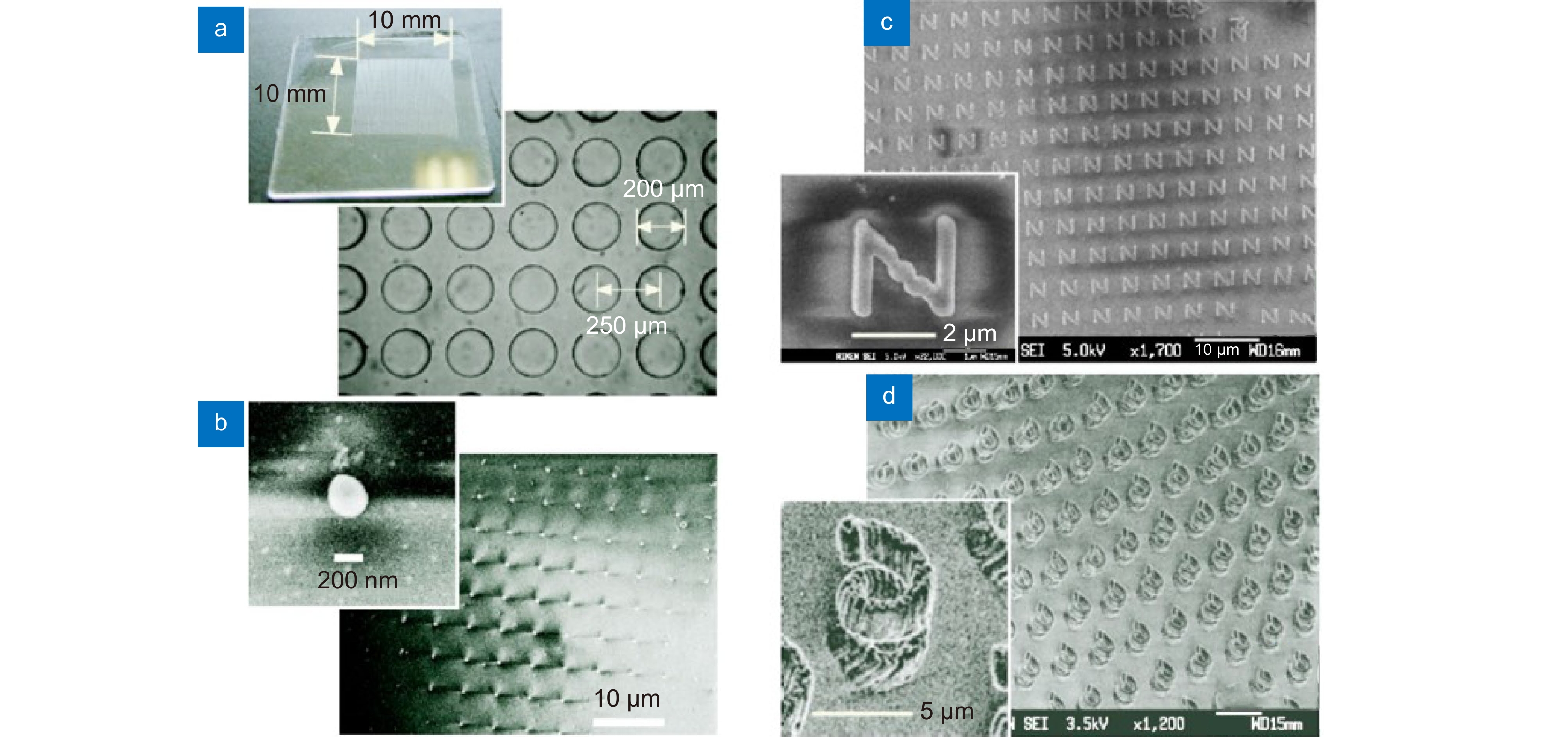
Figure 6.
(a) The overall appearance and optical microscopic image of MLA; (b) SEM of the photopolymerized resin voxels on glass substrate; (c) The 2D array structure of 277 ‘N’ microletters fabricated by 28 foci;(d) The fabricated 3D microspring array[65]
-
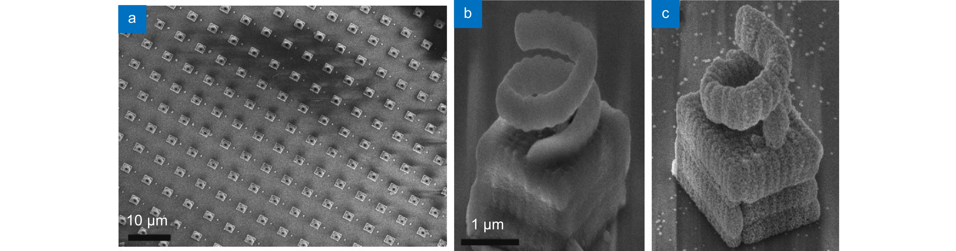
Figure 7.
(a) SEM of 3D periodic structures coated with silver fabricated on a hydrophobic coated glass surface; (b) Enlarged view of a single uncoated polymerized structure composed of a spring on top of a cube; (c) The polymerized structure of (b) with coated silver[66]
-
Figure 8.
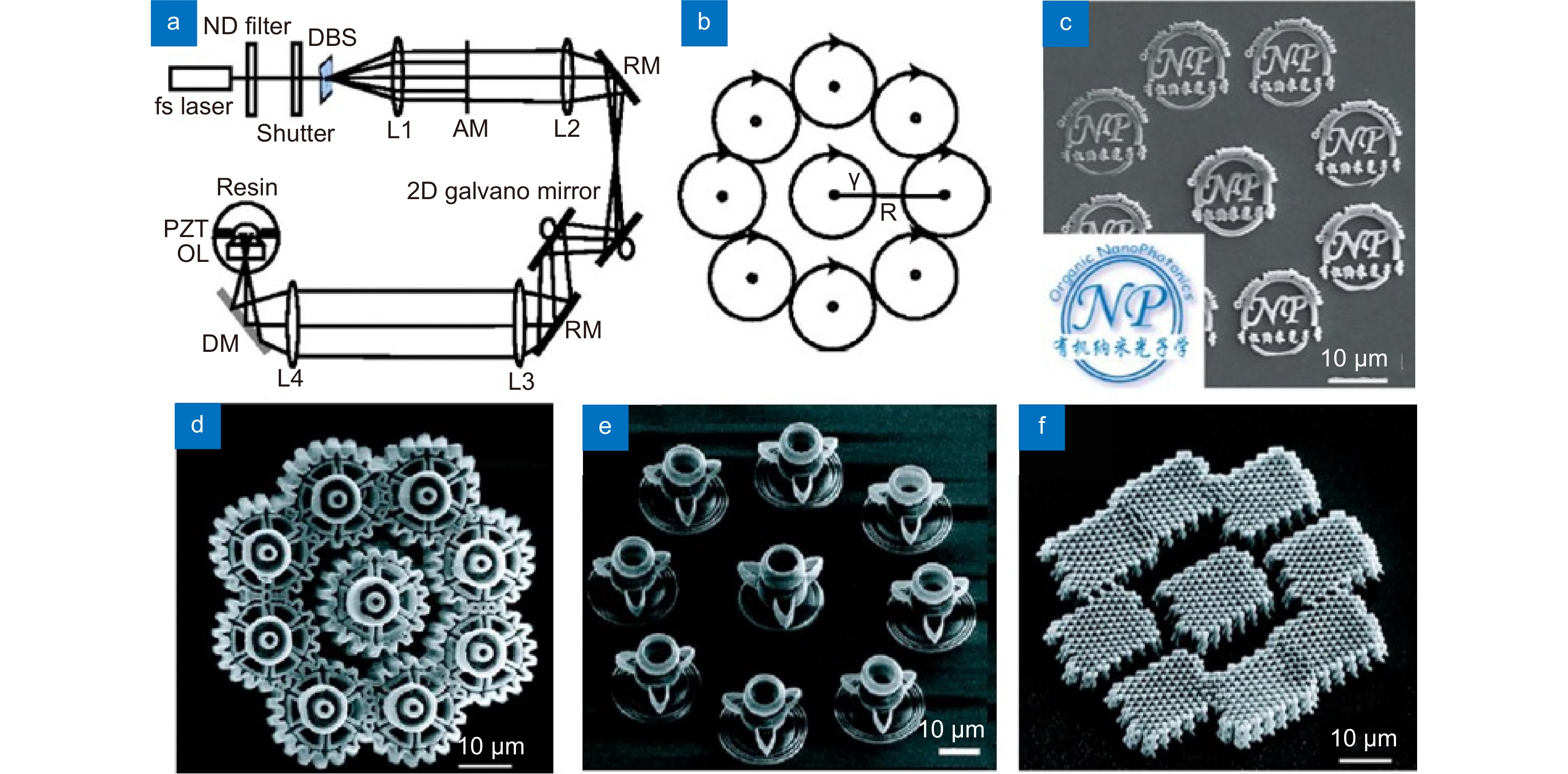
(a) DBS-based multi-photon processing system with multiple femtosecond laser beams; (b) Multi-foci pattern generated by DBS; (c)~(f) The structures of designed Logo, assembled microgear set (diameter 22 μm), 3D microfans, and assembled microgear set fabricated with the optical setup of (a)[72]
-
Figure 9.
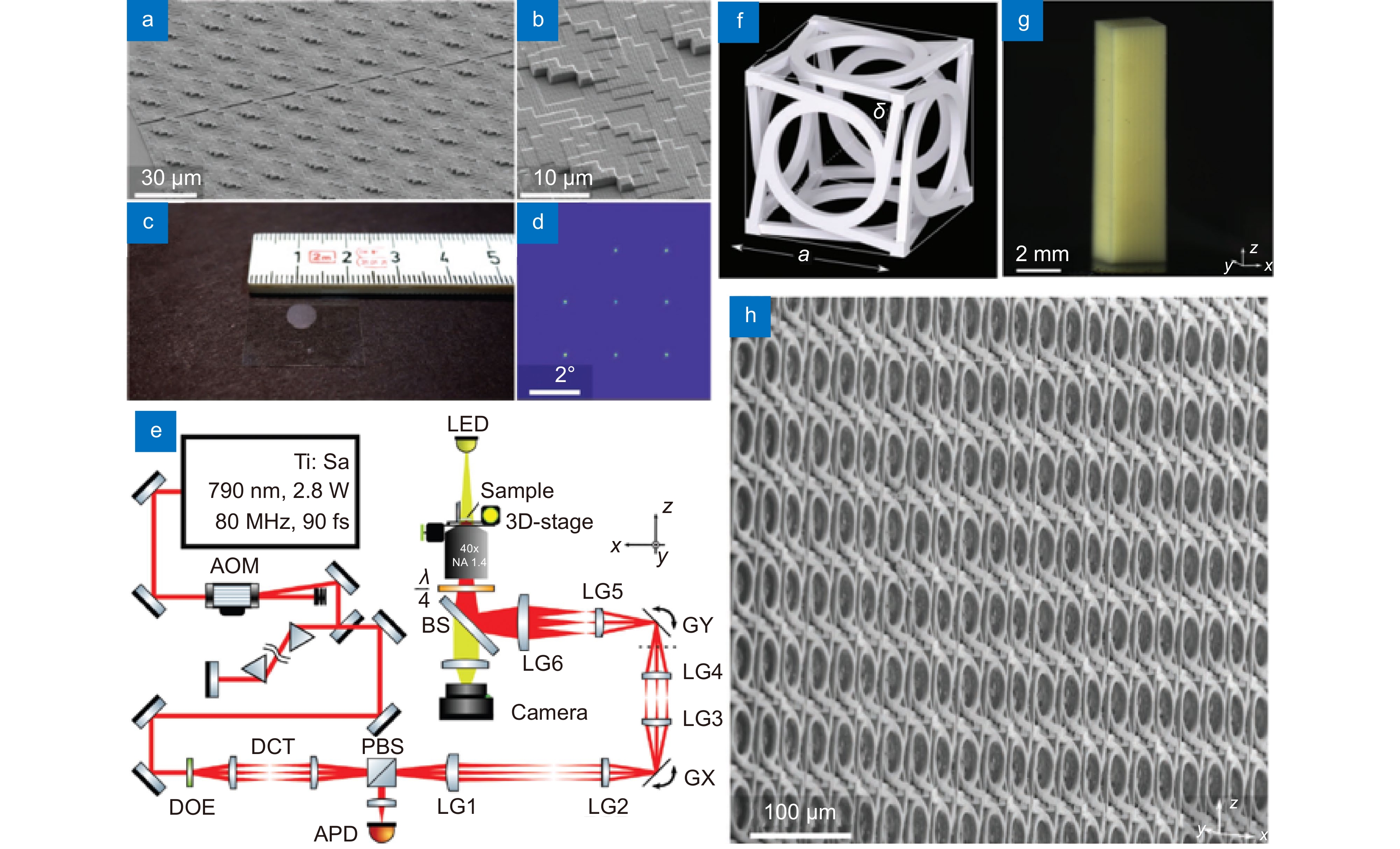
DOE-based mluti-beam parallel femtosecond laser writing. (a) SEM of the DOE surface; (b) Enlarged view of (a); (c) Overall appearance of the DOE; (d) Normalized false-color intensity measurement of the DOE using a CMOS-camera; (e) Parallel 3D two-photon fabricating system based on 3×3 foci generated by DOE; (f) Designed model of the chiral 3D metamaterial cubic cell, a=80 μm; (g) 2.4 mm×2.4 mm×9.6 mm chiral metamaterial structure consisting of 30×30×120=108000 3D cubic cells of (f); (h) Oblique side-view SEM of the structure in (g)73]
-
Figure 10.
(a) The SLM-based multi-foci femtosecond two-photon lithography system; (b) The Venus sculptures fabricated by 4×4 foci; (c) The scaffold for cell cultivation fabricated by 4 foci; (d) 36 microneedles processed by 4 foci[74]
-
Figure 11.
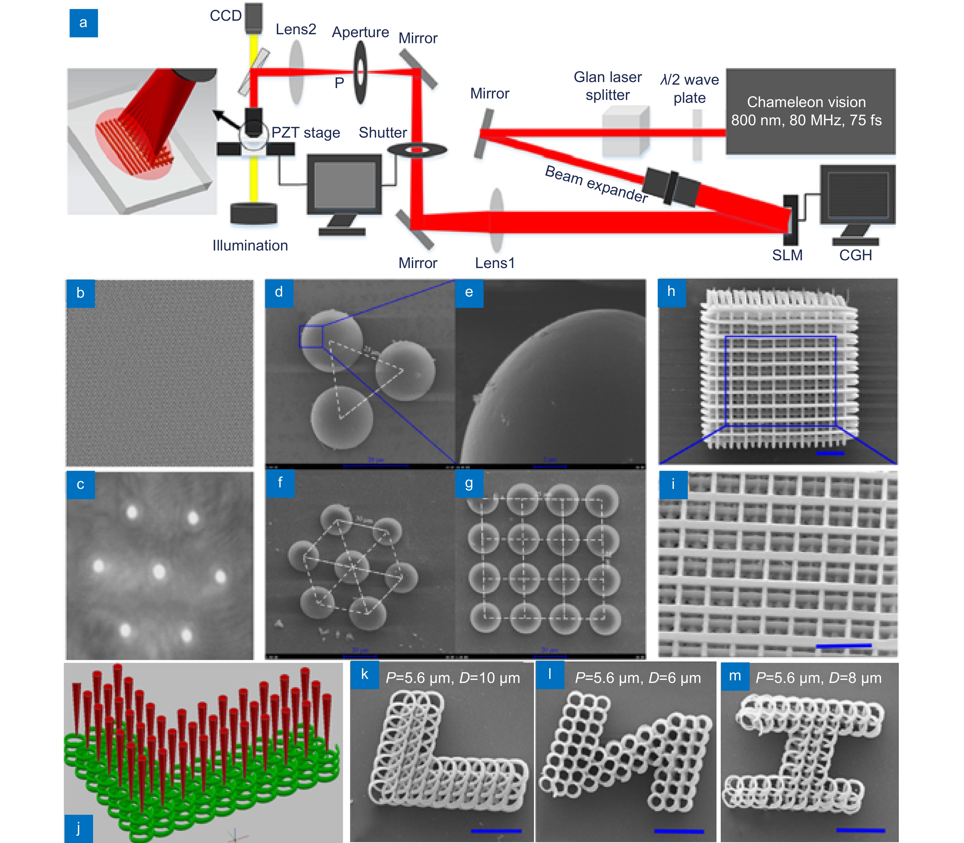
(a) The SLM-based multi-foci femtosecond laser parallel writing system; (b)~(c) The hologram loaded in SLM and the generated 7 foci pattern, respectively; (d)~(g) Microlens arrays fabricated by SLM with 3 foci, 7 foci, and 4×4 foci respectively; (h)~(i) The overall image and enlarged view of the 3D woodpile photonic structure fabricated by 10 foci; (j) Illustration of the multi-foci parallel fabrication process with the spiral scanning strategy; (k)~(m) 3D spiral photonic structures of ‘L’, ‘Z’, and ‘H’ fabricated by the multi-beam scanning way of (j). The foci pitch is 5.6 μm and the diameters of scanning spiral are 10 μm, 6 μm, and 8 μm, respectively[75]
-
Figure 12.
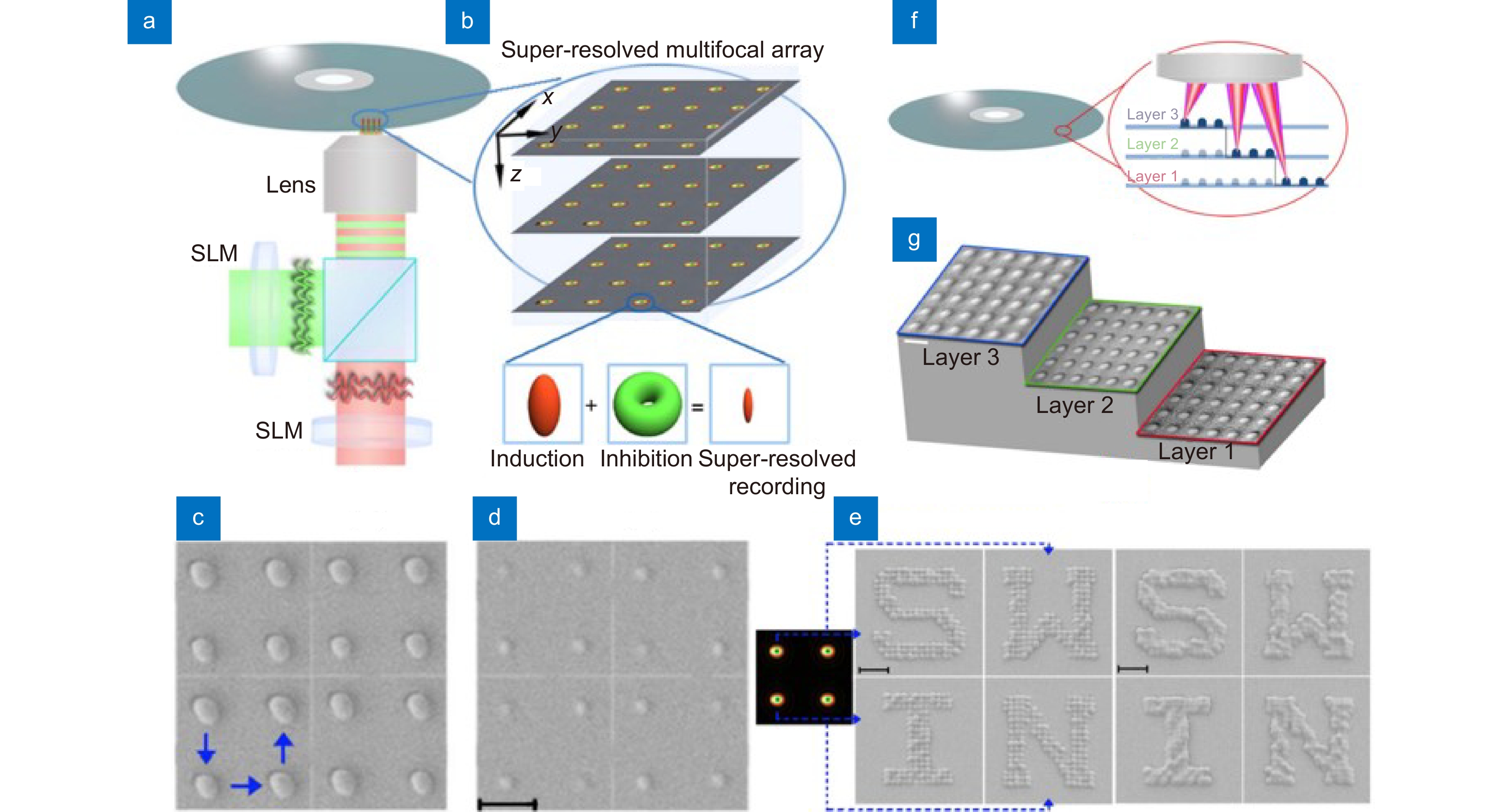
(a) Phase modulation scheme based on two synchronized SLMs; (b) Illustration of the 3D PPI array through duplicating the 2×2 parallel PPI foci; (c) The dot array fabricated with femtosecond foci. The blue arrows indicate the scanning route; (d) The dot array fabricated by PPI foci with inhibition power of 210 mW. Scale bar: 500 nm; (e) SEM of the fabricated letters by 2 × 2 PPI foci (left) and the femtosecond multifocal array (right). Each letter is processed respectively by one focus of the 2×2 multifocal array. Scale bars: 1 μm; (f) The scheme for parallelized PPI 3D writing on different layers with interval of 1.5 μm; (g) 3D dots with interval of 200 nm and size of 80 nm on three different layers which are fabricated by the PPI multifocal array [76]
-
Figure 13.
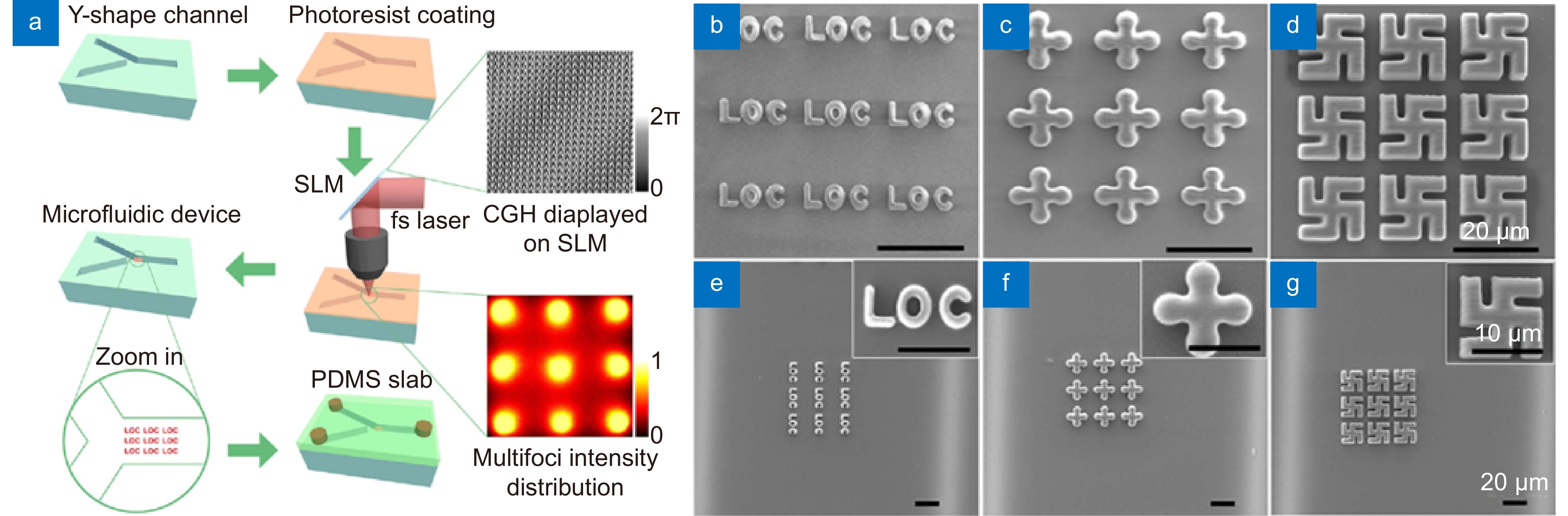
(a) Illustration of fabricating integrated miniaturized structure inside a ‘Y’ shape microchannel by parallel femtosecond multiple foci; (b)~(g) the structures with patterns of ‘LOC’ characters, ‘Cross’ and ‘Svastika’ fabricated on the substrate surface (b)~(d) and in the channel (e)~(g) respectively [77]
-
Figure 14.
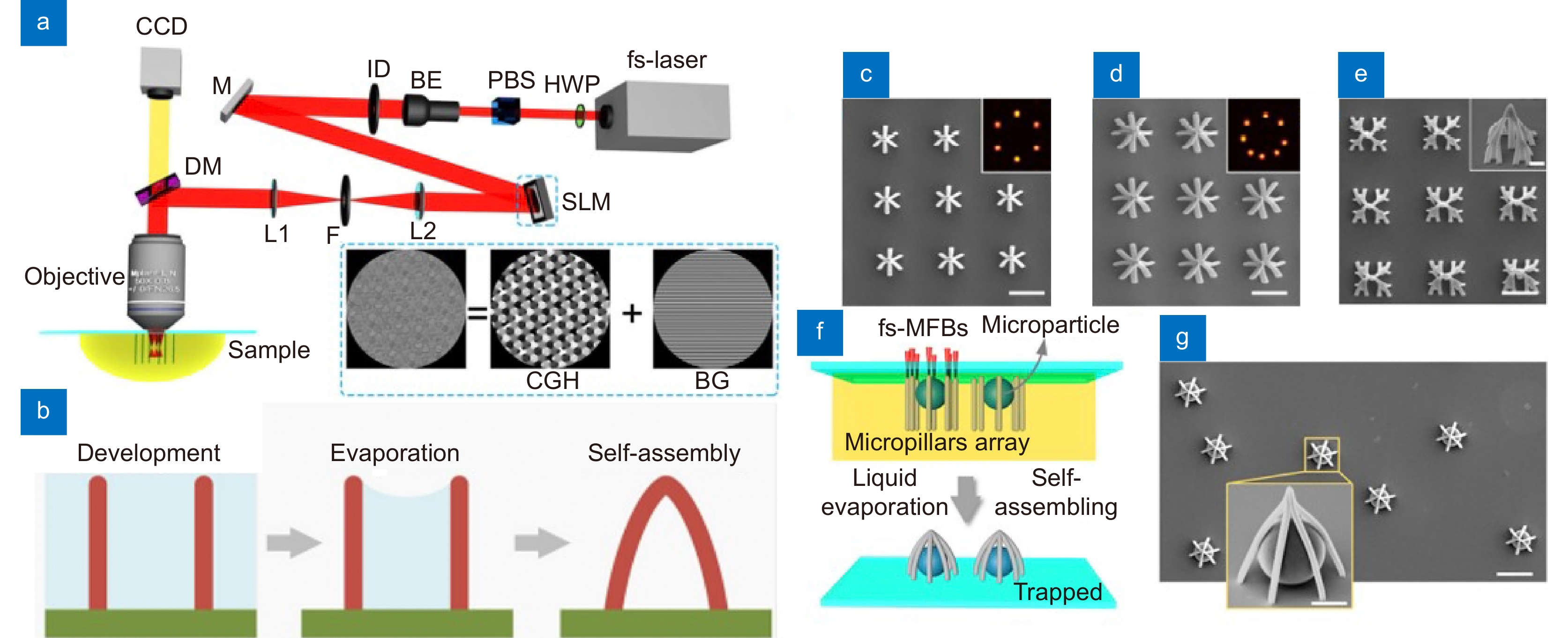
(a) The configuration of SLM-based multi-foci parallel writing system for micropillar fabrication. The inset illustrates the design of CGH; (b) The schematic diagram of self-assembly structure formation by capillary force on micropillars; (c)~(e) Diverse micro-assemblies with 6, 8, and 12 micropillars respectively fabricated by foci array with different beam quantity and distribution.Scale bar: 2 μm; (f)~(g) In-situ trapping of microparticles by the micro-assemblies fabricated with six-foci beams[78]
-
Figure 15.
(a) Optical configuration of DMD-based multi-foci femtosecond laser parallel writing system; (b) Designed laser scanning trajectories, laser writing process, and SEMs of the fabricated woodpile structures with single-focus, two-foci, and three-foci writing respectively. Scale bar: 10 μm[79]
-
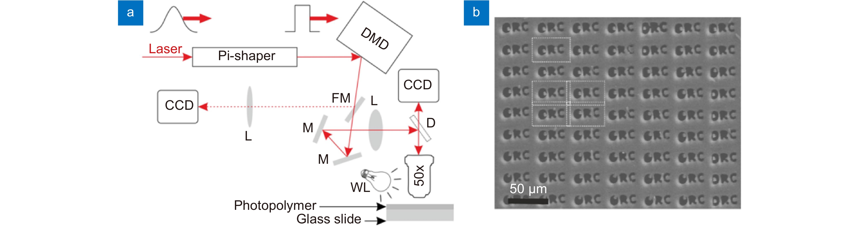
Figure 16.
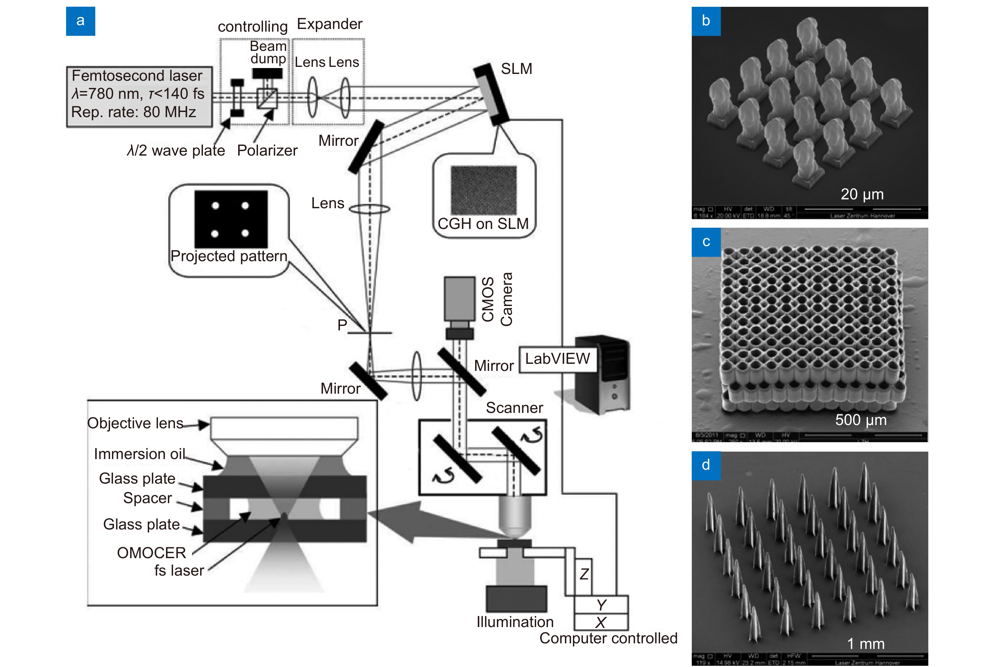
(a) Schematic diagram of the DMD-based femtosecond laser projection lithography system; (b) Large-scale periodic microstructures of ‘ORC’ letters fabricated by DMD once projection[80]
-
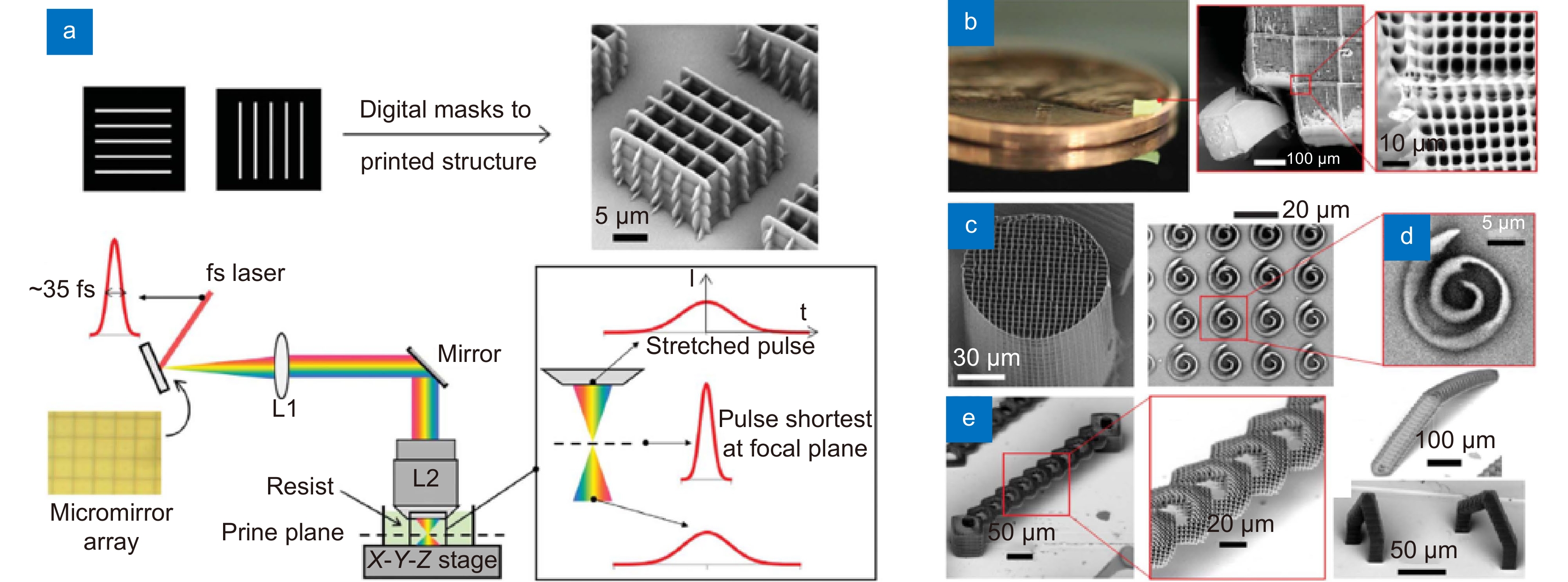
Figure 17.
(a) Schematic diagram of DMD-based projection system using the spatial and temporal focusing of femtosecond laser; (b) 2.2 mm×2.2 mm×0.25 mm cube supported on a U.S. penny fabricated in 8 min 20 s; (c) Fabricated 3D micropillar stacked with2D layers; (d) Spiral structures through once projection within several millisecond; (e) Overhanging 3D structures[30]
-
Figure 18.
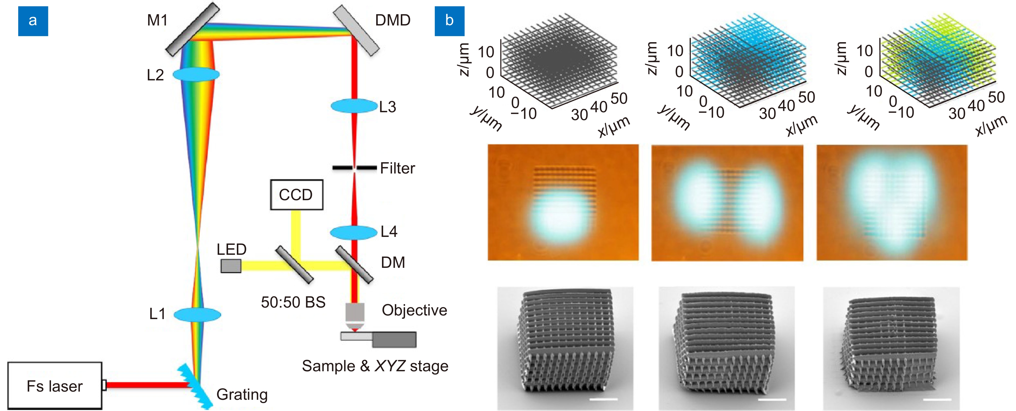
(a) Schematic diagram of femtosecond laser direct writing. The optical intensity distribution at the focal plane is a round point; (b) Schematic diagram of single-exposure holographic femtosecond laser direct patterning. The optical intensity distribution at the defocused plane is a complex pattern ‘H’ designed by computer generated hologram (CGH). However, the distribution shows low signal-to-noise and leads to low surface quality in fabricating micro/nanostructures; (c) Multiexposure holographic femtosecond laser direct patterning. The optical intensity distribution at the defocused plane is a complex pattern ‘H’ designed by multi-CGH with different phases. Due to the improved strategy, the distribution shows high signal-to-noise and thus high quality micro/nanostructures will be realized[81-82]
-
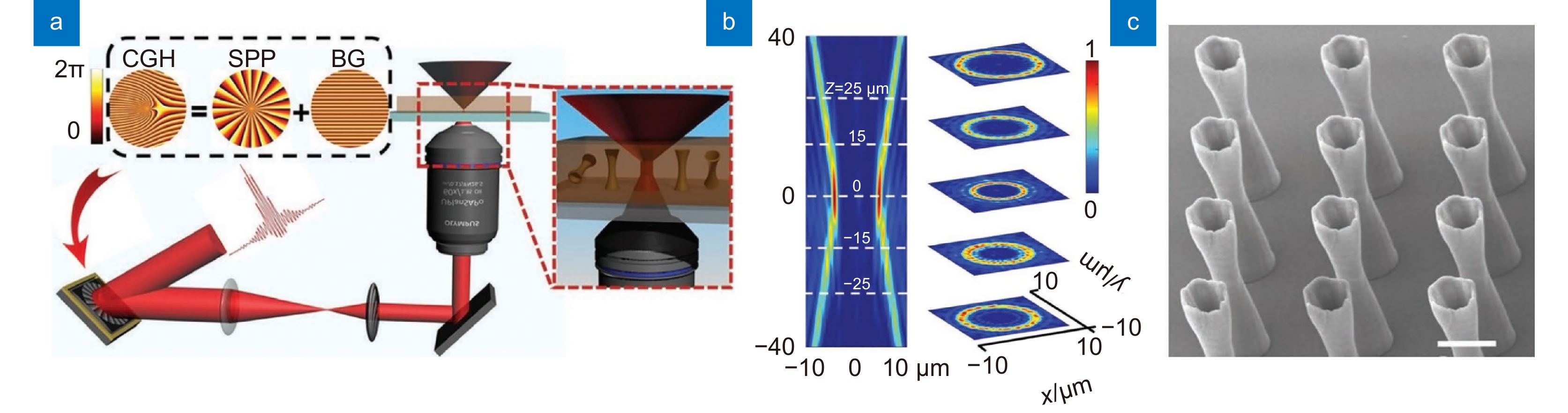
Figure 19.
(a) Experimental setup for single exposure fabrication of microtubes; (b) Calculated light intensity distribution at the focal region in the propagation direction; (c) SEM of microtubes[89]
-
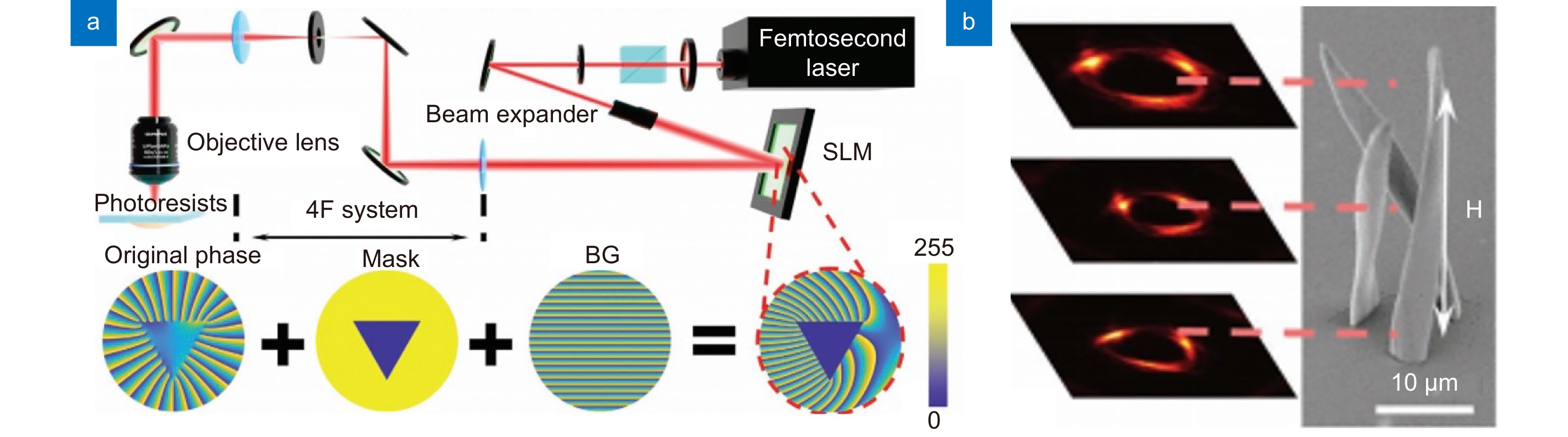
Figure 20.
(a) Experimental setup for the fabrication of 3D chiral microstructures by single exposure; (b) The spatial intensity distribution of the modulated beam and the electron microscopy of the writing results[90]
- Figure .


