
 E-mail Alert
 RSS
RSS
| Citation: |
Luan M L, Zheng J X, Sun X C, et al. Liquid-assisted laser fabrication of hard materials and applications[J]. Opto-Electron Eng, 2023, 50(3): 220328. doi: 10.12086/oee.2023.220328

|
Liquid-assisted laser fabrication of hard materials and applications
-
Abstract
Due to the stable mechanical and chemical properties, excellent photoelectric properties, and other advantages, hard and brittle materials have been widely used in aerospace, the photoelectric industry, and other fields. Laser fabrication is an ideal technology for hard and brittle materials processing due to its high precision, high energy, and non-contact properties. In order to achieve the removal of hard and brittle materials, high laser energy is usually required, resulting in low structural accuracy and poor surface quality. This review introduces the advances of liquid-assisted laser fabrication technology in the processing of hard and brittle materials, introduces the principles of three liquid-assisted laser fabrication technologies, and compares their advantages and disadvantages. The effects of different processing technologies, types of auxiliary liquids, and processing parameters on the quality of different materials were summarized in detail. The main applications of liquid-assisted laser fabrication technology were summarized, and the existing problems and potential development of this technology were discussed. -

-
References
[1] Gao B, Chen T, Khuat V, et al. Fabrication of grating structures on silicon carbide by femtosecond laser irradiation and wet etching[J]. Chin Opt Lett, 2016, 14(2): 021407. doi: 10.3788/COL201614.021407 [2] Bharadwaj V, Wang Y C, Fernandez T T, et al. Femtosecond laser written diamond waveguides: a step towards integrated photonics in the far infrared[J]. Opt Mater, 2018, 85: 183−185. doi: 10.1016/j.optmat.2018.08.062 [3] Cao J J, Hou Z S, Tian Z N, et al. Bioinspired zoom compound eyes enable variable-focus imaging[J]. ACS Appl Mater Interfaces, 2020, 12(9): 10107−10117. doi: 10.1021/acsami.9b21008 [4] Feng S C, Zhang R, Huang C Z, et al. An investigation of recast behavior in laser ablation of 4H-silicon carbide wafer[J]. Mater Sci Semicond Process, 2020, 105: 104701. doi: 10.1016/j.mssp.2019.104701 [5] Saini S K, Dubey A K. Study of material characteristics in laser trepan drilling of ZTA[J]. J Manuf Process, 2019, 44: 349−358. doi: 10.1016/j.jmapro.2019.06.017 [6] Chang H F, Yeung W K, Kao W C, et al. Surface micromachining on a polymethylmethacrylate substrate using visible laser-induced backside wet etching with a KMnO4 solution as an absorber[J]. J Laser Appl, 2020, 32(2): 022014. doi: 10.2351/1.5114659 [7] Feng W H, Guo J, Yan W J, et al. Deep channel fabrication on copper by multi-scan underwater laser machining[J]. Opt Laser Technol, 2019, 111: 653−663. doi: 10.1016/j.optlastec.2018.10.046 [8] Kim K, Song M K, Lee S J, et al. Fundamental study on underwater cutting of 50 mm-thick stainless steel plates using a fiber laser for nuclear decommissioning[J]. Appl Sci, 2022, 12(1): 495. doi: 10.3390/app12010495 [9] Frias Batista L M, Nag A, Meader V K, et al. Generation of nanomaterials by reactive laser-synthesis in liquid[J]. Sci China Phys Mech Astron, 2022, 65(7): 274202. doi: 10.1007/s11433-021-1835-x [10] Wang J, Niino H, Yabe A. One-step microfabrication of fused silica by laser ablation of an organic solution[J]. Appl Phys A, 1999, 68(1): 111−113. doi: 10.1007/s003390050863 [11] Tian W T, Wang Z W, Wang C J, et al. Effects of bubble behaviors in femtosecond laser machining of silicon wafer in liquids[J]. J Manuf Process, 2022, 83: 502−511. doi: 10.1016/j.jmapro.2022.09.024 [12] Derrien T J Y, Koter R, Krüger J, et al. Plasmonic formation mechanism of periodic 100-nm-structures upon femtosecond laser irradiation of silicon in water[J]. J Appl Phys, 2014, 116(7): 074902. doi: 10.1063/1.4887808 [13] Long J Y, Eliceiri M, Vangelatos Z, et al. Early dynamics of cavitation bubbles generated during ns laser ablation of submerged targets[J]. Opt Express, 2020, 28(10): 14300−14309. doi: 10.1364/OE.391584 [14] Kalus M R, Bärsch N, Streubel R, et al. How persistent microbubbles shield nanoparticle productivity in laser synthesis of colloids - quantification of their volume, dwell dynamics, and gas composition[J]. Phys Chem Chem Phys, 2017, 19(10): 7112−7123. doi: 10.1039/C6CP07011F [15] Zhang D S, Li Z G, Sugioka K. Laser ablation in liquids for nanomaterial synthesis: diversities of targets and liquids[J]. J Phys Photonics, 2021, 3(4): 042002. doi: 10.1088/2515-7647/AC0BFD [16] Zhang D S, Li Z G, Liang C H. Diverse nanomaterials synthesized by laser ablation of pure metals in liquids[J]. Sci China Phys Mech Astron, 2022, 65(7): 274203. doi: 10.1007/s11433-021-1860-x [17] Chen L W, Hong M H. Functional nonlinear optical nanoparticles synthesized by laser ablation[J]. Opto-Electron Sci, 2022, 1(5): 210007. doi: 10.29026/oes.2022.210007 [18] Hoppius J S, Maragkaki S, Kanitz A, et al. Optimization of femtosecond laser processing in liquids[J]. Appl Surf Sci, 2019, 467–468: 255−260. doi: 10.1016/j.apsusc.2018.10.121 [19] Guo Y, Qiu P, Xu S L, et al. Laser-induced microjet-assisted ablation for high-quality microfabrication[J]. Int J Extrem Manuf, 2022, 4(3): 035101. doi: 10.1088/2631-7990/ac6632 [20] Ren N F, Xia K B, Yang H Y, et al. Water-assisted femtosecond laser drilling of alumina ceramics[J]. Ceram Int, 2021, 47(8): 11465−11473. doi: 10.1016/j.ceramint.2020.12.274 [21] Zhang D S, Ranjan B, Tanaka T, et al. Underwater persistent bubble-assisted femtosecond laser ablation for hierarchical micro/nanostructuring[J]. Int J Extrem Manuf, 2020, 2(1): 015001. doi: 10.1088/2631-7990/ab729f [22] Zhang D S, Wu L C, Ueki M, et al. Femtosecond laser shockwave peening ablation in liquids for hierarchical micro/nanostructuring of brittle silicon and its biological application[J]. Int J Extrem Manuf, 2020, 2(4): 045001. doi: 10.1088/2631-7990/abb5f3 [23] Wang J, Niino H, Yabe A. Micromachining of transparent materials with super-heated liquid generated by multiphotonic absorption of organic molecule[J]. Appl Surf Sci, 2000, 154–155: 571−576. doi: 10.1016/S0169-4332(99)00462-6 [24] Cao X W, Chen Q D, Fan H, et al. Liquid-assisted femtosecond laser precision-machining of silica[J]. Nanomaterials (Basel), 2018, 8(5): 287. doi: 10.3390/nano8050287 [25] Sun X Y, Yu J L, Hu Y W, et al. Study on ablation threshold of fused silica by liquid-assisted femtosecond laser processing[J]. Appl Opt, 2019, 58(33): 9027−9032. doi: 10.1364/AO.58.009027 [26] Kopitkovas G, Lippert T, David C, et al. Fabrication of beam homogenizers in quartz by laser micromachining[J]. J Photochem Photobiol A: Chem, 2004, 166(1–3): 135–140.https://doi.org/10.1016/j.jphotochem.2004.05.001. [27] Zhigalina O M, Khmelenin D N, Atanova A V, et al. A nanoscale modification of materials at thermoplasmonic laser-induced backside wet etching of sapphire[J]. Plasmonics, 2020, 15(3): 599−608. doi: 10.1007/s11468-019-01091-9 [28] Long J Y, Zhou C X, Cao Z Q, et al. Incubation effect during laser-induced backside wet etching of sapphire using high-repetition-rate near-infrared nanosecond lasers[J]. Opt Laser Technol, 2019, 109: 61−70. doi: 10.1016/j.optlastec.2018.07.066 [29] Olenin A Y, Lisichkin G V. Metal nanoparticles in condensed media: preparation and the bulk and surface structural dynamics[J]. Russ Chem Rev, 2011, 80(7): 605−630. doi: 10.1070/RC2011v080n07ABEH004201 [30] Ding X M, Sato T, Kawaguchi Y, et al. Laser-induced backside wet etching of sapphire[J]. Jpn J Appl Phys, 2003, 42(2B): L176−L178. doi: 10.1143/JJAP.42.L176 [31] Xie X Z, Huang X D, Jiang W, et al. Three dimensional material removal model of laser-induced backside wet etching of sapphire substrate with CuSO4 solutions[J]. Opt Laser Technol, 2017, 89: 59−68. doi: 10.1016/j.optlastec.2016.09.031 [32] Yan T Y, Ji L F, Hong M H. Backside wet etching of sapphire substrate by laser-induced carbothermal reduction[J]. Opt Laser Technol, 2022, 149: 107900. doi: 10.1016/J.OPTLASTEC.2022.107900 [33] Luong K P, Tanabe-Yamagishi R, Yamada N, et al. Laser-assisted wet etching of silicon back surfaces using 1552 nm femtosecond laser[J]. Int J Electr Mach, 2020, 25: 7. doi: 10.2526/ijem.25.7 [34] Deng C, Ki H. Tunable wetting surfaces with interacting cavities via femtosecond laser patterning and wet etching[J]. J Appl Phys, 2020, 128(1): 015306. doi: 10.1063/5.0011885 [35] Wang S K, Zhang F, Yang Q, et al. Chalcogenide glass IR artificial compound eyes based on femtosecond laser microfabrication[J]. Adv Mater Technol, 2022, 8(2): 2200741. doi: 10.1002/admt.202200741 [36] Kim Y S, Kim J, Choe J S, et al. Semiconductor microlenses fabricated by one-step wet etching[J]. IEEE Photonics Technol Lett, 2000, 12(5): 507−509. doi: 10.1109/68.841268 [37] Atuchin V V, Soldatenkov I S, Kirpichnikov A V, et al. Multilevel kinoform microlens arrays in fused silica for high-power laser optics[J]. Proc SPIE, 2004, 5481: 43−46. doi: 10.1117/12.558295 [38] Cao X W, Lu Y M, Fan H, et al. Wet-etching-assisted femtosecond laser holographic processing of a sapphire concave microlens array[J]. Appl Opt, 2018, 57(32): 9604−9608. doi: 10.1364/AO.57.009604 [39] Gao B, Chen T, Chen Y, et al. Fabrication of through micro-hole arrays in silicon using femtosecond laser irradiation and selective chemical etching[J]. Chin Phys Lett, 2015, 32(10): 107901. doi: 10.1088/0256-307X/32/10/107901 [40] Khuat V, Ma Y C, Si J H, et al. Fabrication of through holes in silicon carbide using femtosecond laser irradiation and acid etching[J]. Appl Surf Sci, 2014, 289: 529−532. doi: 10.1016/j.apsusc.2013.11.030 [41] Meng X W, Yang Q, Chen F, et al. Fabrication of 3D solenoid microcoils in silica glass by femtosecond laser wet etch and microsolidics[J]. Proc SPIE, 2015, 9449: 94493N. doi: 10.1117/12.2075880 [42] Wang C W, Yang L, Zhang C C, et al. Multilayered skyscraper microchips fabricated by hybrid "all-in-one" femtosecond laser processing[J]. Microsyst Nanoeng, 2019, 5: 17. doi: 10.1038/s41378-019-0056-3 [43] Cho C S, Kong D, Kim B. Wet/dry etching combined microtextured structures for high-efficiency solar cells[J]. Micro Nano Lett, 2015, 10(10): 528−532. doi: 10.1049/mnl.2015.0182 [44] Sugioka K, Masuda M, Hongo T, et al. Three-dimensional microfluidic structure embedded in photostructurable glass by femtosecond laser for lab-on-chip applications[J]. Appl Phys A, 2004, 79(4–6): 815−817. doi: 10.1007/s00339-004-2569-2 [45] Wang B X, Qi J Y, Lu Y M, et al. Rapid fabrication of smooth micro-optical components on glass by etching-assisted femtosecond laser modification[J]. Materials (Basel), 2022, 15(2): 678. doi: 10.3390/MA15020678 [46] Sugioka K, Cheng Y. Integrated microchips for biological analysis fabricated by femtosecond laser direct writing[J]. MRS Bull, 2011, 36(12): 1020−1027. doi: 10.1557/mrs.2011.274 [47] Xu J, Wu D, Hanada Y, et al. Electrofluidics fabricated by space-selective metallization in glass microfluidic structures using femtosecond laser direct writing[J]. Lab Chip, 2013, 13(23): 4608−4616. doi: 10.1039/c3lc50962a [48] Wu D, Wu S Z, Xu J, et al. Hybrid femtosecond laser microfabrication to achieve true 3D glass/polymer composite biochips with multiscale features and high performance: the concept of ship-in-a-bottle biochip[J]. Laser Photon Rev, 2014, 8(3): 458−467. doi: 10.1002/lpor.201400005 [49] Bian H, Shan C, Liu K Y, et al. A miniaturized Rogowski current transducer with wide bandwidth and fast response[J]. J Micromech Microeng, 2016, 26(11): 115015. doi: 10.1088/0960-1317/26/11/115015 [50] Ehrhardt M, Lorenz P, Han B, et al. Laser-induced backside wet etching of SiO2 with a visible ultrashort laser pulse by using KMnO4 solution as an absorber liquid[J]. J Laser Micro/Nanoeng, 2018, 13(2): 47−54. doi: 10.2961/jlmn.2018.02.0001 [51] Kwon K K, Kim H, Kim T, et al. High aspect ratio channel fabrication with near-infrared laser-induced backside wet etching[J]. J Mater Process Technol, 2020, 278: 116505. doi: 10.1016/j.jmatprotec.2019.116505 [52] Li X Y, Li R Y, Yu Z, et al. Deepening of nanograting structures on Si by a two-step laser spatial-selective amorphization strategy combined with chemical etching[J]. Appl Surf Sci, 2022, 589: 152965. doi: 10.1016/J.APSUSC.2022.152965 [53] Zhou S P, Li X W, Huang J, et al. Fabrication of nanogap structures through spatially shaped femtosecond laser modification with the assistance of wet chemical etching[J]. Opt Lett, 2021, 46(15): 3560−3563. doi: 10.1364/OL.431385 [54] Hao B, Liu H W. , Chen F, et al. Versatile route to gapless microlens arrays using laser-tunable wet-etched curved surfaces[J]. Opt Express, 2012, 20(12): 12939−12948. doi: 10.1364/OE.20.012939 [55] Li X W, Xie Q, Jiang L, et al. Controllable Si (100) micro/nanostructures by chemical-etching-assisted femtosecond laser single-pulse irradiation[J]. Appl Phys Lett, 2017, 110(18): 181907. doi: 10.1063/1.4982790 [56] Ito Y, Chiah S Y, Luong K P, et al. Formation of fine periodic structures on back surface of Si substrate by a femtosecond laser at 1552 nm[J]. J Laser Micro/Nanoeng, 2020, 15(2): 111−117. doi: 10.2961/jlmn.2020.02.2006 [57] Zhang D S, Li X Z, Fu Y, et al. Liquid vortexes and flows induced by femtosecond laser ablation in liquid governing formation of circular and crisscross LIPSS[J]. Opto-Electron Adv, 2022, 5(2): 210066. doi: 10.29026/oea.2022.210066 [58] Zhang D S, Ranjan B, Tanaka T, et al. Carbonized hybrid micro/nanostructured metasurfaces produced by femtosecond laser ablation in organic solvents for biomimetic antireflective surfaces[J]. ACS Appl Nano Mater, 2020, 3(2): 1855−1871. doi: 10.1021/acsanm.9b02520 [59] Zhang D S, Sugioka K. Hierarchical microstructures with high spatial frequency laser induced periodic surface structures possessing different orientations created by femtosecond laser ablation of silicon in liquids[J]. Opto-Electron Adv, 2019, 2(3): 190002. doi: 10.29026/oea.2019.190002 [60] Ali N, Bashir S, Umm-I-Kalsoom, et al. Effect of liquid environment on the titanium surface modification by laser ablation[J]. Appl Surf Sci, 2017, 405: 298−307. doi: 10.1016/j.apsusc.2017.02.047 [61] Sato T, Kurosaki R, Kawaguchi Y, et al. Fabrication of multiple slanted microstructures on silica glass by laser-induced backside wet etching[J]. J Laser Micro/Nanoeng, 2010, 5(3): 256−262. doi: 10.2961/jlmn.2010.03.0014 [62] Zhao T, Zhuo M, Zhou X, et al. Fused silica gyroscope resonator manufactured with femtosecond laser assisted wet etching[J]. J Microelectromech Syst, 2022, 31(3): 315−317. doi: 10.1109/JMEMS.2022.3154890 [63] Skora J L, Gaiffe O, Bargiel S, et al. High-fidelity glass micro-axicons fabricated by laser-assisted wet etching[J]. Opt Express, 2022, 30(3): 3749−3759. doi: 10.1364/OE.446740 [64] Zhang F, Wang C, Yin K, et al. Quasi-periodic concave microlens array for liquid refractive index sensing fabricated by femtosecond laser assisted with chemical etching[J]. Sci Rep, 2018, 8(1): 2419. doi: 10.1038/s41598-018-20807-1 [65] Sun X Y, Zheng J F, Liang C, et al. Improvement of rear damage of thin fused silica by liquid-assisted femtosecond laser cutting[J]. Appl Phys A, 2019, 125(7): 461. doi: 10.1007/s00339-019-2754-y [66] Ehrhardt M, Raciukaitis G, Gecys P, et al. Microstructuring of fused silica by laser-induced backside wet etching using picosecond laser pulses[J]. Appl Surf Sci, 2010, 256(23): 7222−7227. doi: 10.1016/j.apsusc.2010.05.055 [67] Böhme R, Pissadakis S, Ehrhardt M, et al. Ultra-short laser processing of transparent material at the interface to liquid[J]. J Phys D Appl Phys, 2006, 39(7): 1398−1404. doi: 10.1088/0022-3727/39/7/010 [68] Shao Z Q, Wu Y L, Wang S, et al. All-sapphire-based fiber-optic pressure sensor for high-temperature applications based on wet etching[J]. Opt Express, 2021, 29(3): 4139−4146. doi: 10.1364/OE.417246 [69] Li Q K, Cao J J, Yu Y H, et al. Fabrication of an anti-reflective microstructure on sapphire by femtosecond laser direct writing[J]. Opt Lett, 2017, 42(3): 543−546. doi: 10.1364/OL.42.000543 [70] Pissadakis S, Böhme R, Zimmer K. Sub-micron periodic structuring of sapphire by laser induced backside wet etching technique[J]. Opt Express, 2007, 15(4): 1428−1433. doi: 10.1364/OE.15.001428 [71] Ehrhardt M, Raciukaitis G, Gecys P, et al. Laser-induced backside wet etching of fluoride and sapphire using picosecond laser pulses[J]. Appl Phys A, 2010, 101(2): 399−404. doi: 10.1007/s00339-010-5833-7 [72] Zhou S K, Shen L, Wang F J, et al. High-aspect-ratio ZnSe microstructure generated by spatially shaped femtosecond laser writing assisted with wet chemical etching[J]. Opt Laser Technol, 2022, 147: 107687. doi: 10.1016/j.optlastec.2021.107687 [73] Bischof D, Kahl M, Michler M. Laser-assisted etching of borosilicate glass in potassium hydroxide[J]. Opt Mater Express, 2021, 11(4): 1185−1195. doi: 10.1364/OME.417871 [74] Seo J M, Kwon K K, Song K Y, et al. Deposition of durable micro copper patterns into glass by combining laser-induced backside wet etching and laser-induced chemical liquid phase deposition methods[J]. Materials (Basel), 2020, 13(13): 2977. doi: 10.3390/ma13132977 [75] Zhang D S, Gökce B, Sommer S, et al. Debris-free rear-side picosecond laser ablation of thin germanium wafers in water with ethanol[J]. Appl Surf Sci, 2016, 367: 222−230. doi: 10.1016/j.apsusc.2016.01.071 [76] Miyata Y, Nakamukai Y, Azevedo C T, et al. Photoetching method that provides improved silicon-on-insulator layer thickness uniformity in a defined area[J]. Microelectron Eng, 2017, 180: 93−95. doi: 10.1016/j.mee.2017.06.008 [77] Duan M M, Wu J J, Zhang Y B, et al. Ultra-low-reflective, self-cleaning surface by fabrication dual-scale hierarchical optical structures on silicon[J]. Coatings, 2021, 11(12): 1541. doi: 10.3390/coatings11121541 [78] Kawaguchi Y, Sato T, Narazaki A, et al. Rapid prototyping of silica glass microstructures by the LIBWE method: fabrication of deep microtrenches[J]. J Photochem Photobiol A:Chem, 2006, 182(3): 319−324. doi: 10.1016/j.jphotochem.2006.05.033 [79] Koker L, Kolasinski K W. Photoelectrochemical etching of Si and porous Si in aqueous HF[J]. Phys Chem Chem Phys, 2000, 2(2): 277−281. doi: 10.1039/a908383i [80] Gabouze N, Belhousse S, Outemzabet R. Chemical etching of mono and poly-crystalline silicon in HF/K2Cr2O7/H2O solutions[J]. Acta Phys Slovaca, 2003, 53(3): 207−214. [81] Romano L, Vila-Comamala J, Jefimovs K, et al. High-aspect-ratio grating microfabrication by platinum-assisted chemical etching and gold electroplating[J]. Adv Eng Mater, 2020, 22(10): 2000258. doi: 10.1002/adem.202000258 [82] Immanuel P N, Chiang C C, Lee T H, et al. Utilization of low wavelength laser linking with electrochemical etching to produce nano-scale porous layer on p-type silicon wafer with high luminous flux[J]. ECS J Solid State Sci Technol, 2021, 10(1): 016003. doi: 10.1149/2162-8777/abdc4b [83] Chen L, Cao K Q, Li Y L, et al. Large-area straight, regular periodic surface structures produced on fused silica by the interference of two femtosecond laser beams through cylindrical lens[J]. Opto-Electron Adv, 2021, 4(12): 200036. doi: 10.29026/oea.2021.200036 [84] Chen F, Liu H W, Yang Q, et al. Maskless fabrication of concave microlens arrays on silica glasses by a femtosecond-laser-enhanced local wet etching method[J]. Opt Express, 2010, 18(19): 20334−20343. doi: 10.1364/OE.18.020334 [85] Kim J, Kim S I, Joung Y H, et al. Two-step hybrid process of movable part inside glass substrate using ultrafast laser[J]. Micro Nano Syst Lett, 2021, 9(1): 16. doi: 10.1186/S40486-021-00142-3 [86] Paiè P, Bragheri F, Di Carlo D, et al. Particle focusing by 3D inertial microfluidics[J]. Microsyst Nanoeng, 2017, 3: 17027. doi: 10.1038/micronano.2017.27 [87] He F, Cheng Y, Xu Z Z, et al. Direct fabrication of homogeneous microfluidic channels embedded in fused silica using a femtosecond laser[J]. Opt Lett, 2010, 35(3): 282−284. doi: 10.1364/OL.35.000282 [88] Jipa F, Iosub S, Calin B, et al. High repetition rate UV versus VIS picosecond laser fabrication of 3D microfluidic channels embedded in photosensitive glass[J]. Nanomaterials (Basel), 2018, 8(8): 583. doi: 10.3390/nano8080583 [89] Capuano L, Berenschot J W, Tiggelaar R M, et al. Fabrication of microstructures in the bulk and on the surface of sapphire by anisotropic selective wet etching of laser-affected volumes[J]. J Micromech Microeng, 2022, 32(12): 125003. doi: 10.1088/1361-6439/ac9911 [90] Hua J G, Liang S Y, Chen Q D, et al. Free-form micro-optics out of crystals: femtosecond laser 3D sculpturing[J]. Adv Funct Mater, 2022, 32(26): 2200255. doi: 10.1002/adfm.202200255 [91] Gao S, Li Z Z, Hu Z Y, et al. Diamond optical vortex generator processed by ultraviolet femtosecond laser[J]. Opt Lett, 2020, 45(9): 2684−2687. doi: 10.1364/OL.391598 [92] Liu X Q, Zhang Y L, Li Q K, et al. Biomimetic sapphire windows enabled by inside-out femtosecond laser deep-scribing[J]. PhotoniX, 2022, 3(1): 1. doi: 10.1186/s43074-022-00047-3 [93] Masuda M, Sugioka K, Cheng Y, et al. Direct fabrication of freely movable microplate inside photosensitive glass by femtosecond laser for lab-on-chip application[J]. Appl Phys A, 2004, 78(7): 1029−1032. doi: 10.1007/s00339-003-2447-3 [94] Kim S, Kim J, Joung Y H, et al. Optimization of selective laser-induced etching (SLE) for fabrication of 3D glass microfluidic device with multi-layer micro channels[J]. Micro Nano Syst Lett, 2019, 7(1): 15. doi: 10.1186/s40486-019-0094-5 [95] Shan C, Yang Q, Bian H, et al. Fabrication of three-dimensional microvalves of internal nested structures inside fused silica[J]. Micromachines (Basel), 2021, 12(1): 43. doi: 10.3390/MI12010043 [96] Liao Y, Song J X, Li E, et al. Rapid prototyping of three-dimensional microfluidic mixers in glass by femtosecond laser direct writing[J]. Lab Chip, 2012, 12(4): 746−749. doi: 10.1039/c2lc21015k [97] 张超, 李敏, 叶柏臣, 等. 飞秒激光时空整形的电子动态调控微孔加工[J]. 光电工程, 2022, 49(2): 210389. doi: 10.12086/oee.2022.210389 Zhang C, Li M, Ye B C, et al. Electrons dynamics control micro-hole drilling using temporally/spatially shaped femtosecond laser[J]. Opto-Electron Eng, 2022, 49(2): 210389. doi: 10.12086/oee.2022.210389 [98] Lu Y M, Duan Y Z, Liu X Q, et al. High-quality rapid laser drilling of transparent hard materials[J]. Opt Lett, 2022, 47(4): 921−924. doi: 10.1364/OL.452530. [99] Madhukar Y K, Mullick S, Nath A K. A study on co-axial water-jet assisted fiber laser grooving of silicon[J]. J Mater Process Technol, 2016, 227: 200−215. doi: 10.1016/j.jmatprotec.2015.08.013 [100] Li W Y, Luo Y, Xiong B, et al. Fabrication of GaN-based ridge waveguides with very smooth and vertical sidewalls by combined plasma dry etching and wet chemical etching[J]. Phys Status Solidi A, 2015, 212(10): 2341−2344. doi: 10.1002/pssa.201532223 [101] Shao Z Q, Wu Y L, Wang S, et al. All-sapphire fiber-optic pressure sensors for extreme harsh environments[J]. Opt Express, 2022, 30(3): 3665−3674. doi: 10.1364/OE.451764 -
Overview
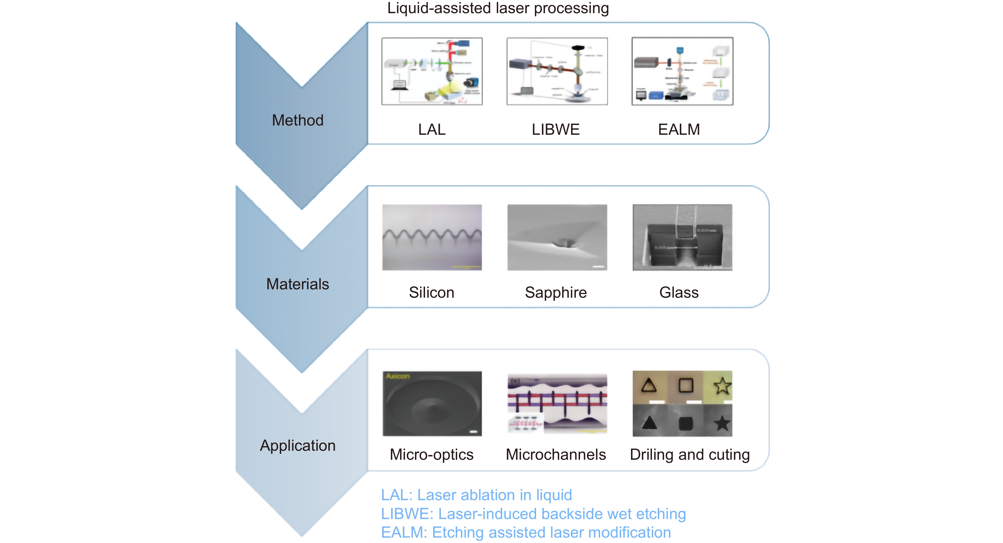
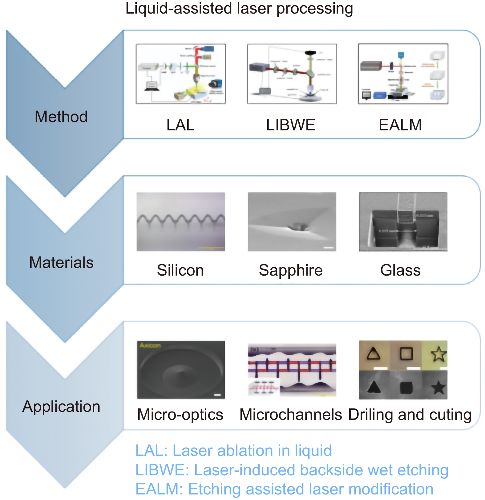
With the development of industry, laser fabrication has become one of the important technologies for welding, cutting, surface processing, and other advanced manufacturing areas. At the same time, the pursuit of structures miniaturization, devices integration, and high precision has put forward more stringent requirements for laser fabrication technologies. Due to the advantages of stable mechanical and chemical properties and unique photoelectric properties, hard and brittle materials have been widely used in aerospace, the photoelectric industry, et al. Laser fabrication is an ideal technology for hard and brittle materials processing due to its high precision, high energy, and non-contact properties. In order to achieve the removal of hard and brittle materials, high laser energy is usually required, resulting in low fabrication accuracy and poor surface quality. As an improved laser processing method, liquid-assisted laser fabrication can effectively improve fabrication accuracy and surface quality. The processing characteristics and material removal principles of three different liquid-assisted laser processing technologies are summarized in this review. According to the different functions of the medium through which the laser penetrates and the kinds of liquid, liquid-assisted laser fabrication technology can be divided into Laser ablation in liquid (LAL), laser-induced backside wet etching (LIBWE), and etching-assisted laser modification (EALM). The auxiliary liquid of Laser ablation in liquid is mostly water, which mainly plays the role of cooling and removing debris. The auxiliary liquids used by laser-induced backside wet etching include organic solvents, acid-base solutions, inorganic salts, and other liquids, which play different roles according to different liquids. The etching-assisted laser modification mainly uses an acid or alkaline solution as an auxiliary liquid to remove laser-modified materials. Different methods and auxiliary liquids have different mechanisms in the methods. Therefore, almost any material can be processed by choosing suitable methods and auxiliary liquids, including photosensitive glass, silicon crystal, sapphire, and other transparent hard brittle materials. Here, we summarize the fabrication technologies and fabrication parameters for different materials. The development and applications of liquid-assisted laser fabrication technologies in the fields of micro-optical components, microfluidic devices, and drilling and cutting are introduced. Finally, the challenges of the technology are discussed.
-
Access History
Figures(9)
Tables(2)
Article Metrics

Export File
Citation
Luan M L, Zheng J X, Sun X C, et al. Liquid-assisted laser fabrication of hard materials and applications[J]. Opto-Electron Eng, 2023, 50(3): 220328. doi: 10.12086/oee.2023.220328
Format
Content
 DownLoad:

-
Figure 1.
Outline of the review about liquid-assisted laser fabrication
-
Figure 2.
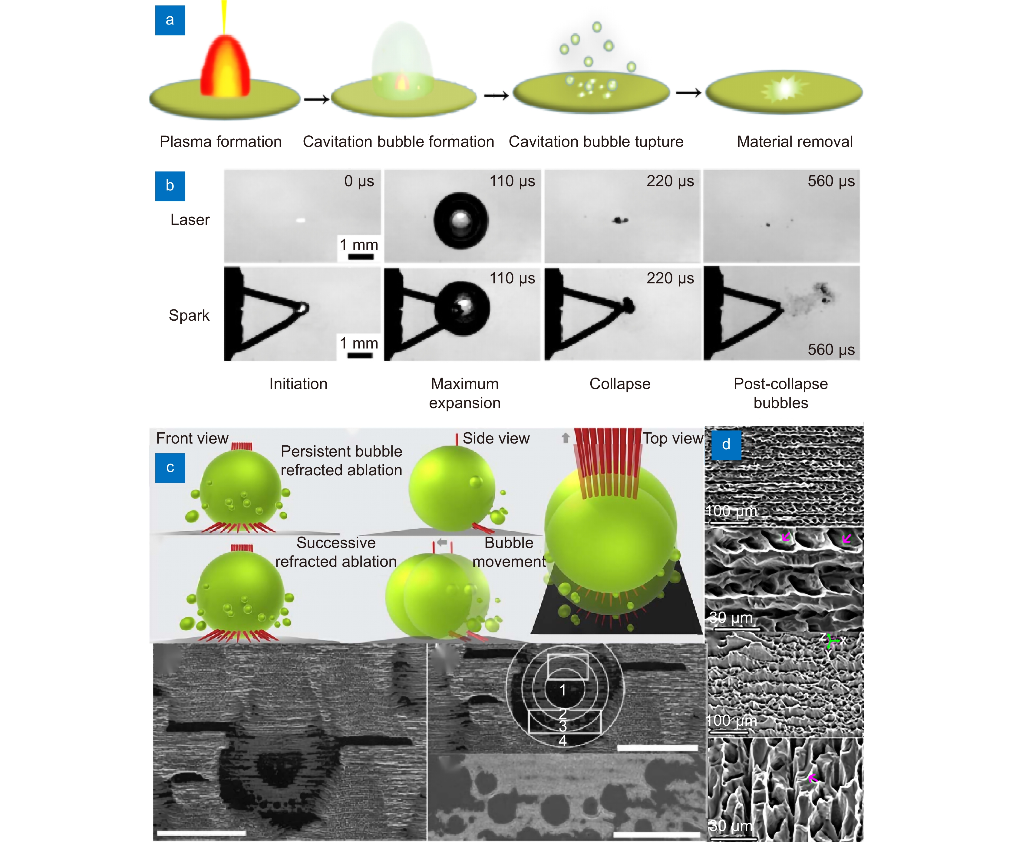
(a) Schematic diagram of liquid phase laser processing; (b) Generation, expansion, collapse, and persistent bubble generation based on cavitation bubbles generated by liquid phase laser ablation [11]; (c) Preparation of tail concentric circle macrostructure based on underwater sustained bubble-assisted femtosecond laser ablation technology[18]; (d) Preparation of porous crack structure based on femtosecond laser impact shot peening liquid ablation technology with different angles and morphology display[19]
-
Figure 3.
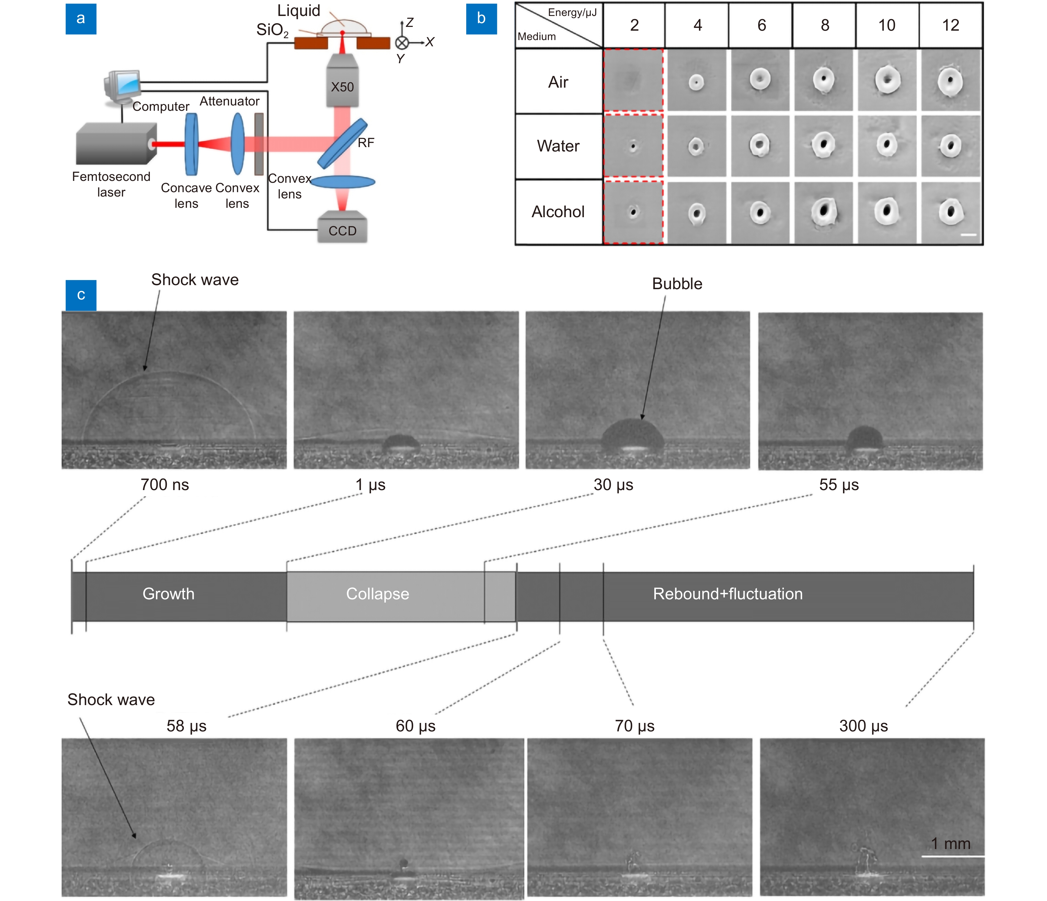
(a) Schematic diagram of laser induced back wet etching optical path system based on femtosecond laser[24] ; (b) Comparison of the morphologies of the holes prepared by laser-induced wet back etching under different environments[25]; (c) Shadow diagram of the hydrodynamics of cavitation bubbles produced by laser-induced wet back etching[26]
-
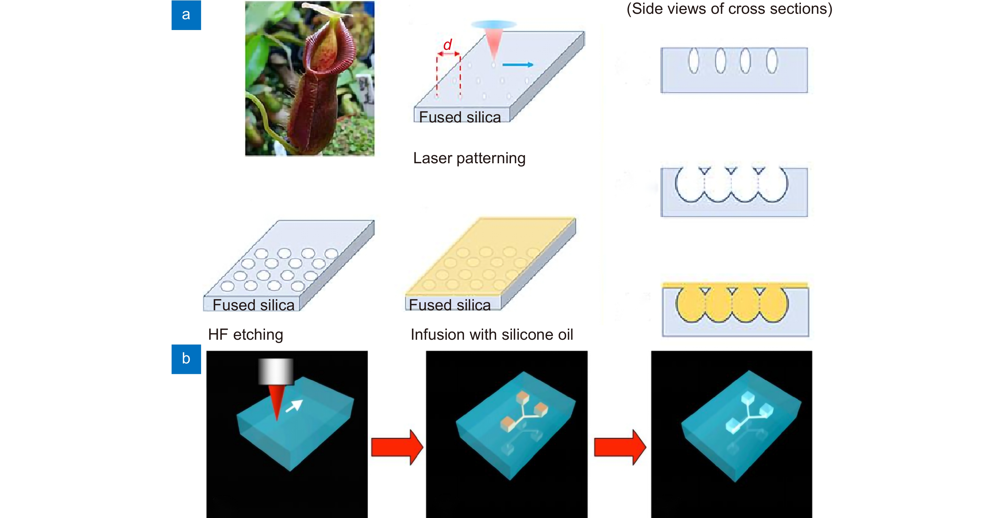
Figure 4.
(a) Flow chart of selective etching using the reaction rates of the auxiliary liquid and the material body and modified area[34]; (b) Flow chart for selective etching using an auxiliary liquid reacting only with the modified region[35]
-
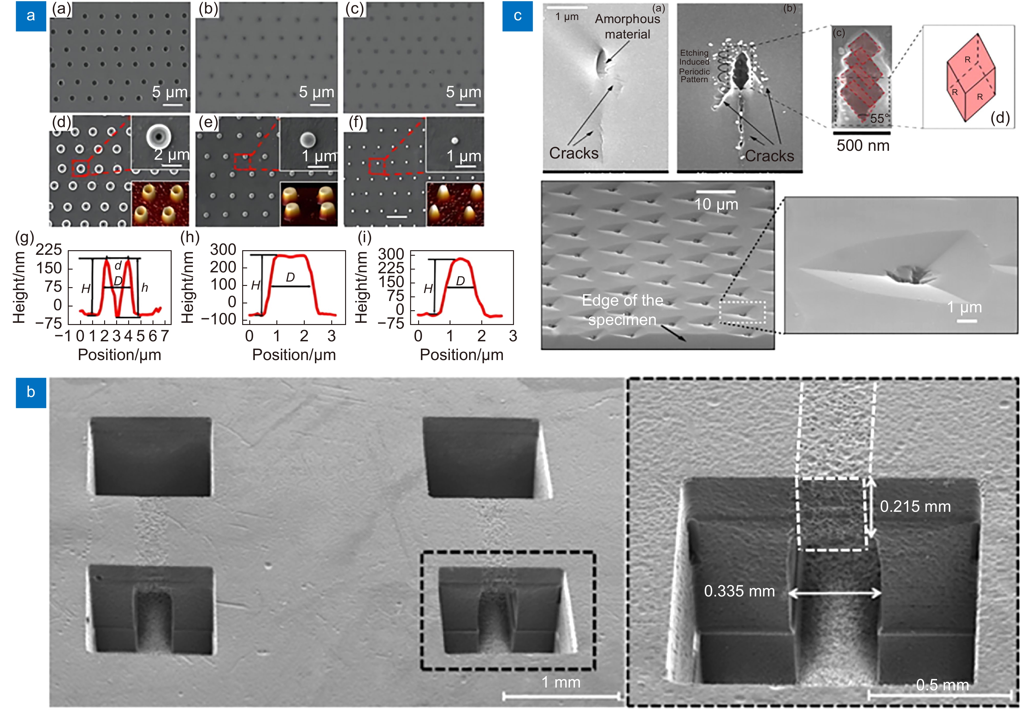
Figure 5.
(a) Three different micro-nano structures are generated on the silicon surface[55]; (b) Microchannel structures are prepared by internal waves in photosensitive glass[88]; (c) Triangular pits prepared by anisotropic etching on the sapphire surface[89]
-
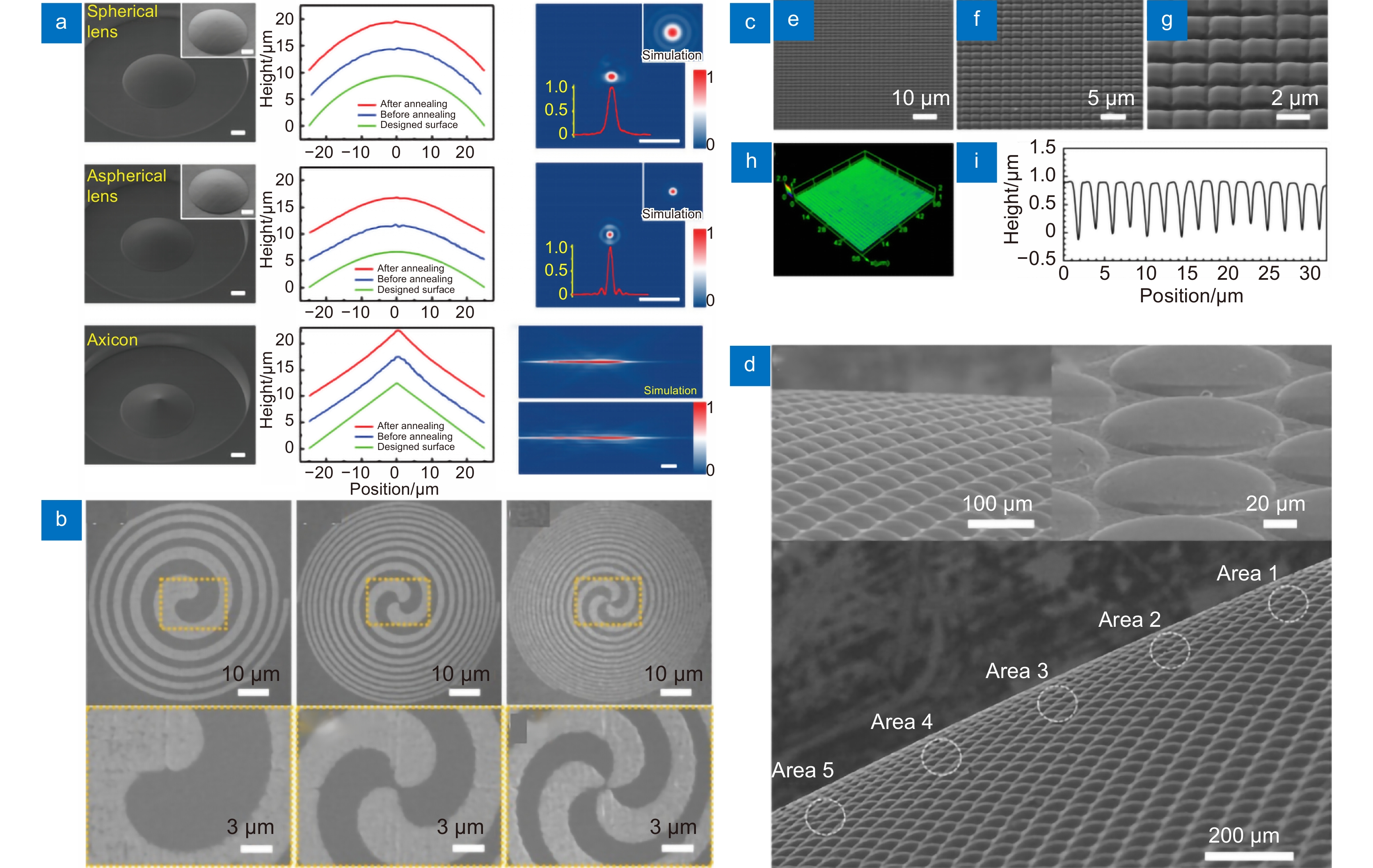
Figure 6.
(a) A single microlens with arbitrary morphology was prepared on the sapphire surface[90]; (b) Preparation of low-light level vortex generators with different morphologies on the diamond surface[91]; (c) The bionic moth-eye anti-reflection structure was prepared uniformly on the surface of the coated sapphire[92]; (d) Highly homogenous artificial compound eye structures prepared on the surface of sulfide[35]
-
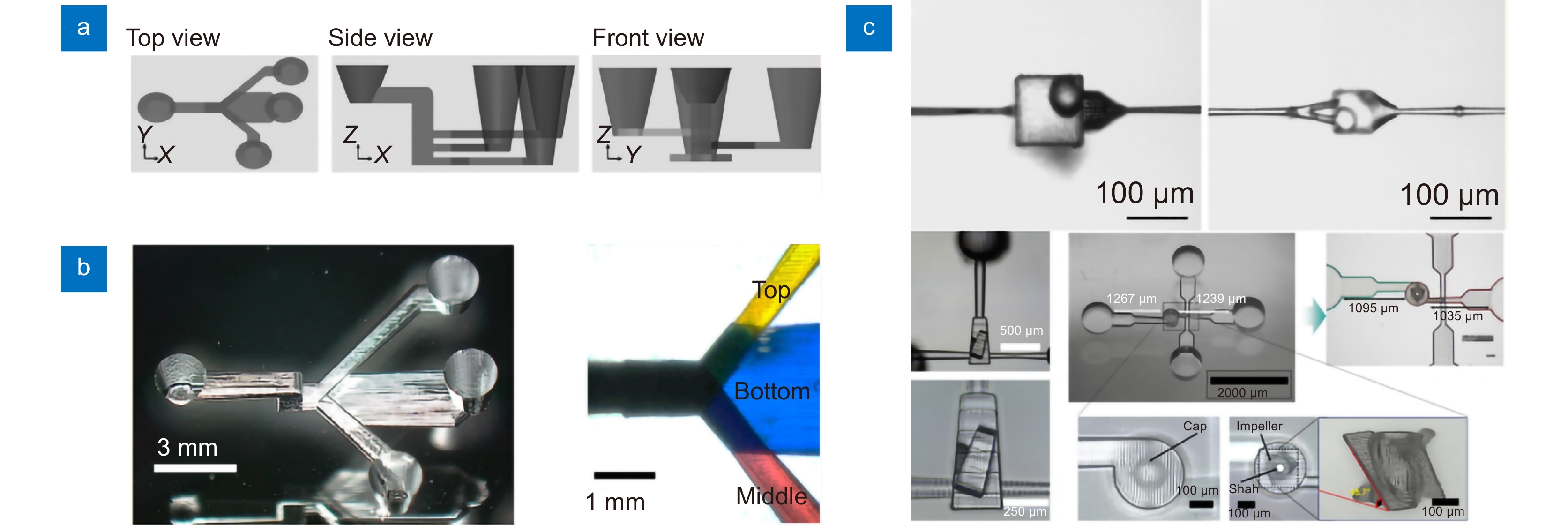
Figure 7.
(a) Three-layer multi-branch microfluidic system[94]; (b) Auxiliary microchannel system with rotating impeller[94]; (c) A nested system structure of microcavities and microspheres that can control the direction of liquid flow[95]
-
Figure 8.
(a) Through hole array prepared by laser-induced micro-jet assisted ablation[19]; (b) Non-taper pores with different morphologies[98]; (c) Microchannel array prepared by laser-induced microjet assisted ablation[19]
- Figure .


